 | ÐлекÑÑоннÑй компоненÑ: SQ6601PT | СкаÑаÑÑ:  PDF PDF  ZIP ZIP |
Äîêóìåíòàöèÿ è îïèñàíèÿ www.docs.chipfind.ru
KSD-I0U001-000
1
SQ6601PT
Off-Line Quasi-Resonance Flyback Switching Regulator
Description
The SQ6601PT is a hybrid IC consists from power MOSFET and a controller IC, designed for Indirect feed-back
Quasi-Resonant (including low frequency PRC)fly-back converter type SMPS (Switching Mode Power Supply)
applications. this IC realizes high efficiency, low noise, downsizing and standardizing of a power supply system
reducing external components count and simplifying the circuit designs. the device is provided in a five pin over-
molded TO-220 style package, affording dielectric isolation without compromising thermal characteristics.
(Note). PRC is abbreviation of "Pulse Ratio Control" (On-width control with fixed OFF-time).
Features
· Quasi-Resonant Operation
· Low-loss, Pulse-Ration-Control standby mode
· Under-voltage lockout with Hysteresis
· Adjustable switching speed for EMI control
· Low start-up circuit current (100uA max)
· Active low-pass filter for stabilizing the operation in case of light load
· Avalanche Energy Guaranteed MOSFET with high VDSS
· Built-in constant voltage drive circuit
· Built-in step drive circuit
· Built-in low frequency PRC mode (20kHz)
· Pulse-by-pulse Overcurrent Protection (OCP)
· Overvoltage Protection with latch mode (OVP)
· Thermal Shutdown with latch mode (TSD)
· Over-molded Five-Pin Package
Ordering Information
Type NO. Marking Package Code
SQ6601PT SQ6601PT TO-220F-5FL
Package Outline
S
S
e
e
m
m
i
i
c
c
o
o
n
n
d
d
u
u
c
c
t
t
o
o
r
r
TO-220 Fullpack (5 Lead)

KSD-I0U001-000
2
Internal Block Diagram
Pin Function
Typical Connection Diagram
Pin Number
Pin Name
Pin Function
1
Drain
Power Switch MOSFET Drain Part
2 Source
Power
Switch
MOSFET Source Part
3
GND
Ground of the Control Section
4
Vcc
Supply Voltage of Output Drive & Control Section
5
FB/OCP
Voltage Mode Control Feedback Signal & Over Current Detection
SQ6601PT
SQ6601PT
KSD-I0U001-000
3
Absolute maximum ratings
(Ta=25°C, Unless otherwise specified)
Characteristic Symbol
Ratings
Unit
Note
Drain Source Voltage
V
DS
650 V
-
Drain Current
I
D
7
A
T
C
= 25
Peak Drain Current
I
DP
28 A
Single
Pulse
Single Pulsed Avalanche Energy
E
AS
640
mJ
L=23mH,V
DD
=100V, I
DP
=7.0A
Control Supply Voltage
V
CC
20 V
-
FB/OCP Voltage Range
FB/OCP
-0.3 ~ +6
V
-
Power Dissipation
P
D
40
W
With infinite heatsink
Thermal Resistance, Junction to Case
R
thJC
3.12
°C
/W
-
Junction Temperature
T
J
150
°C
-
Operating Temperature Range
T
opr
-25
~
+125
°C
-
Storage Temperature Range
T
stg
-55
~
+150
°C
-
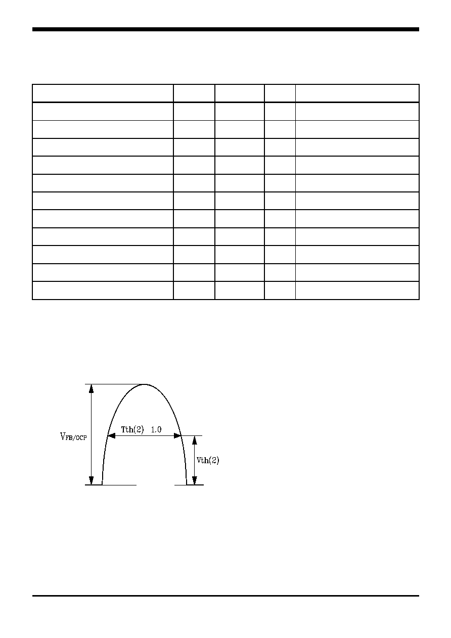
Recommended Operating Conditions
Time for input of quasi resonant signals.
For the Quasi resonant signal inputted to the V
FB/OCP
terminal at the time of quasi resonant operation, the signal
should be wider than Tth(2)
SQ6601PT

KSD-I0U001-000
4
SQ6601PT
Electrical Characteristics
(V
CC
= 11V, Ta = 25
°C
; Unless otherwise specified)
Characteristic Symbol
Test
Conditions
Min.
Typ.
Max.
Units
Start Threshold Voltage
V
TH(ST)
V
CC
Increasing
8.5
9.5
10.5
V
Stop Threshold Voltage
V
TH(SP)
V
CC
decreasing after turn on
start threshold voltage
7.2 8 8.8 V
Start up Supply Current
I
ST
V
CC
= V
TH(ST)
- 0.1V
-
-
100
Operating Supply Current
I
CC
V
FB
= 1V
-
3
7
Dynamic Operating Supply
Current
I
DCC
- -
4
10
Maximum Off Time
t
MAX
Drain waveform high
30
-
60
Minimum Off Time
t
MIN
Drain waveform high
-
-
1.5
Minimum Input Pulse Width
t
MIN(W)
Drain waveform high
-
-
1.0
Over Voltage Threshold
V
OVP
V
CC
Increasing until shut down
output
15.3 17 18.7
V
Latch Release Voltage
V
RE
V
CC
decreasing until latch
releasing
2.5 - 6.0 V
Latch Holding Current
I
CC(RE)
- -
-
400
Feedback Threshold Voltage
V
FB
-
0.68
0.73
0.78
V
Css Snchronized Voltage
V
SYNC
- 1.3
1.45
1.6
V
Feedback Sink Current
I
SINK
V
FB
= 1V
1.2
1.35
1.5
Thermal Shutdown Activation
Temperature
T
J(TSD)
- 140
-
-
Drain-to-Source Breakdown
Voltage
V
DS
I
D
= 300uA
650
-
-
V
Drain Leakage Current
I
DS
V
DS
= 650V
-
-
300
On-State Resistance
R
DS(ON)
I
D
= 3.5A
-
-
1.2
Rise Time
tr
10% to 90%
-
-
250
ns
KSD-I0U001-000
5
SQ6601PT
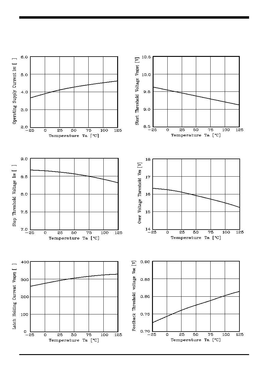
Electrical Characteristic Curves
Fig. 2 V
TH(SP)
vs. Ta
Fig. 6 V
OH
vs.
Ta
Fig. 1 I
CC
vs. Ta
Fig. 3 I
ST
vs. Ta
Fig. 4 V
FB
vs. Ta
Fig. 5 V
TH(ST)
vs. Ta