KST-2125-000
1
STJ828SF
P-Channel Enhancement-Mode MOSFET
S
S
e
e
m
m
i
i
c
c
o
o
n
n
d
d
u
u
c
c
t
t
o
o
r
r
Description
· High speed switching application.
· Analog switch applications.
Features
· -2.5V Gate drive.
· Low threshold voltage : Vth = -0.5~ -1.5V.
· High speed.
Ordering
Information
Type NO.
Marking
Package Code
STJ828SF J28 SOT-23F
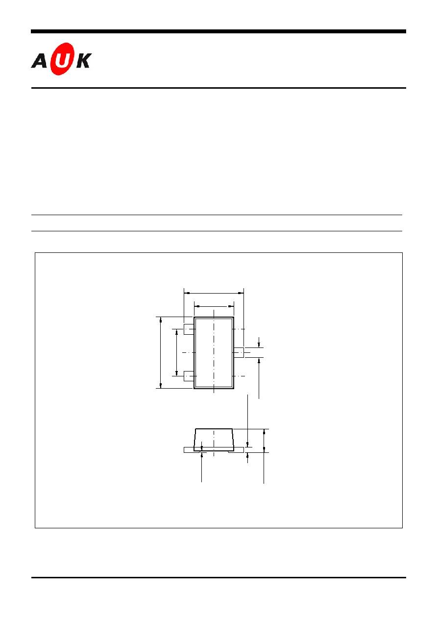
Outline Dimensions unit :
mm
PIN Connections
1. Gate
2. Source
3. Drain
0.
4
±
0.
05
0~0.
1
3
1
2
1.
90 BSC
2.
9
±
0.
1
0.
15
±
0.
05
2.4±0.1
0.
9
±
0.
1
1.6±0.1
KST-2125-000
2
STJ828SF
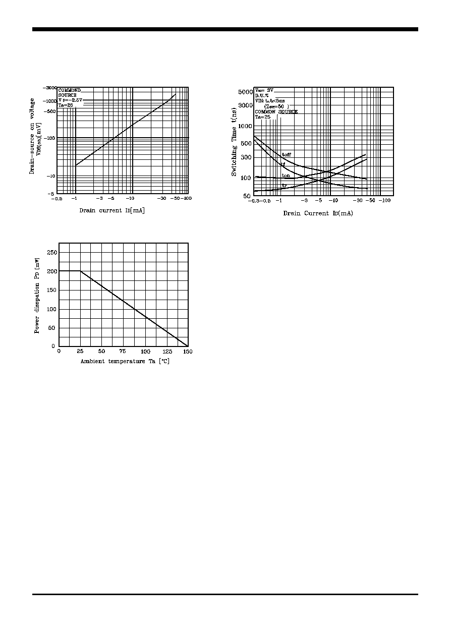
Absolute maximum ratings
(Ta=25
°C)
Characteristic Symbol
Ratings
Unit
Drain-Source voltage
V
DS
-20 V
Gate-Source voltage
V
GSS
±
7
V
DC Drain current
I
D
-50
mA
Drain Power dissipation
P
D
200
mW
Channel temperature
T
ch
150 °C
Storage temperature range
T
stg
-55~150 °C
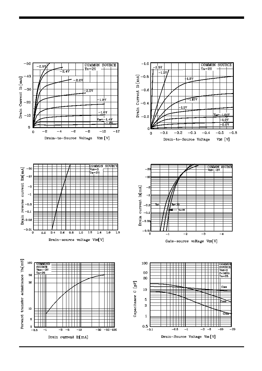
Electrical Characteristics
(Ta=25
°C)
Characteristic Symbol
Test
Condition
Min.
Typ.
Max.
Unit
Drain-Source breakdown voltage
BV
DSS
I
D
=-100µA, V
GS
=0
-20 - V
Gate-Threshold voltage
V
th
I
D
=-0.1mA, V
DS
=-3V -0.5
-
-1.5
V
Drain cut-off current
I
DSS
V
DS
=-20V, V
GS
=0 -
-
-1
µA
Gate leakage current
I
GSS
V
GS
=±7V, V
DS
=0
- - ±1
µA
Drain-Source on-resistance
R
DS(ON)
V
GS
=-2.5V, I
D
=-10mA -
40
Forward transfer admittance
Y
fs
V
DS
=-3V, I
D
=-10mA 15
-
-
mS
Input capacitance
C
iss
V
DS
=-3V, V
GS
=0, f=1MHz
-
10.4
-
pF
Output capacitance
C
oss
V
DS
=-3V, V
GS
=0, f=1MHz
-
8.4
-
pF
Reverse Transfer capacitance
C
rss
V
DS
=-3V, V
GS
=0, f=1MHz
-
2.8
-
pF
Turn-on time
t
ON
V
DD
=-3V, I
D
=-10mA
V
GEN
=0~-2.5V
- 0.15 -
Turn-off time
t
OFF
V
DD
=-3V, I
D
=-10mA
V
GEN
=0~-2.5V
- 0.13 -
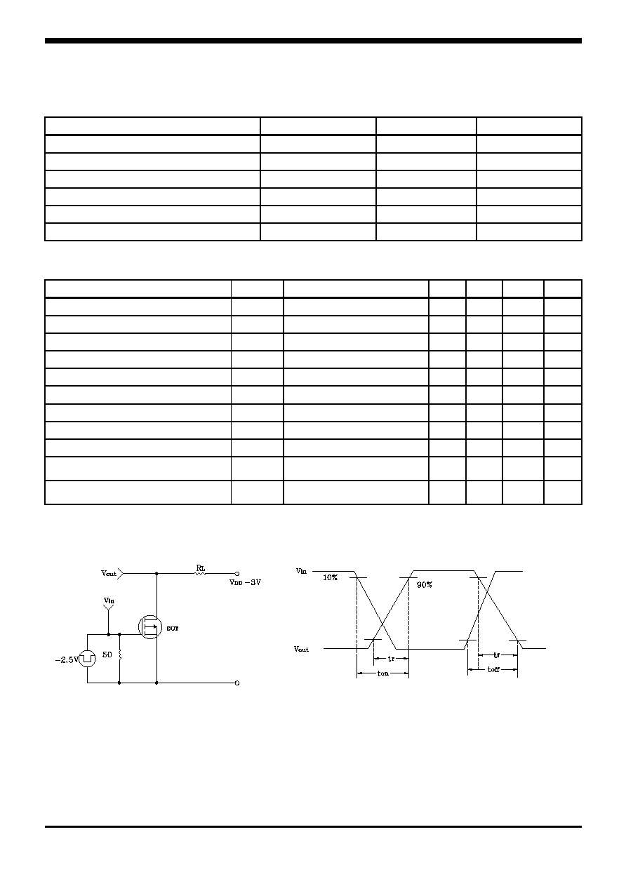
*. Switching Time Test Circuit
=