KSD-T0O014-000
1
STK0160F
Advanced Power MOSFET
S
S
e
e
m
m
i
i
c
c
o
o
n
n
d
d
u
u
c
c
t
t
o
o
r
r
SWITCHING REGULATOR APPLICATIONS
Features
· High Voltage: BV
DSS
=600V(Min.)
· Low C
rss
: C
rss
=4.3pF(Typ.)
· Low gate charge : Qg=4.5nC(Typ.)
· Low R
DS(on)
:R
DS(on)
=9.4(Max.)
Ordering
Information
Type NO.
Marking
Package Code
STK0160F STK0160
TO-220F-3L
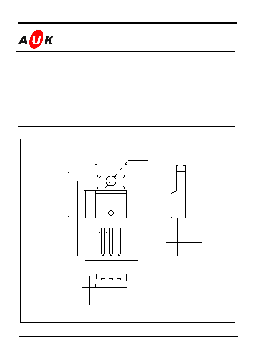
Outline Dimensions unit :
mm
9.80~10.20
15.
40~15.
80
3.05~3.35
12.
20~12.
60
9.
10~9.
30
3.
46 T
y
p
.
1.07 Min.
0.90 Max.
2.54 Typ.
2.54 Typ.
4.
70 Max.
2.
70 Max.
0.
60 Max.
1 2 3
0.60 Max.
2.60~3.00
PIN Connections
1. Gate
2. Drain
3. Source
KSD-T0O014-000
2
STK0160F
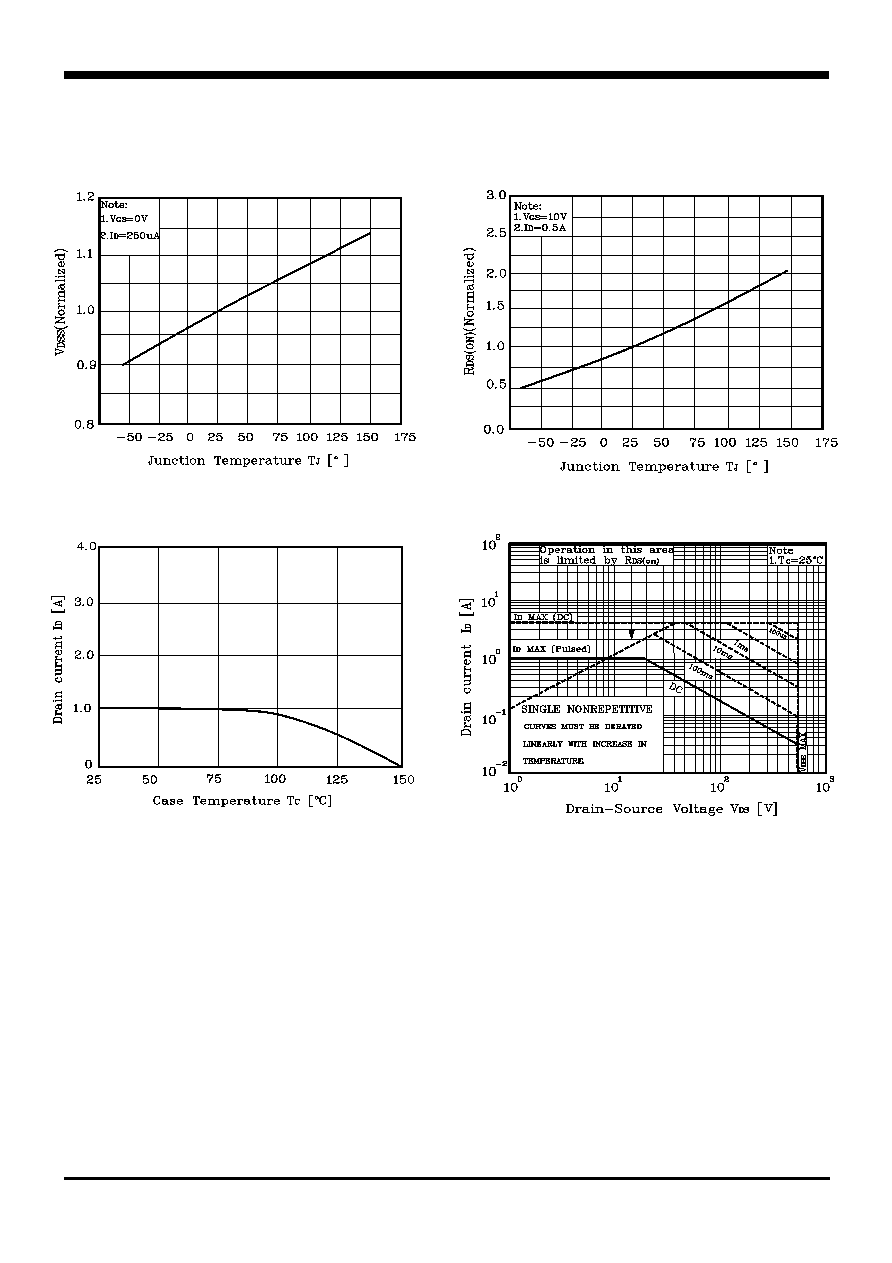
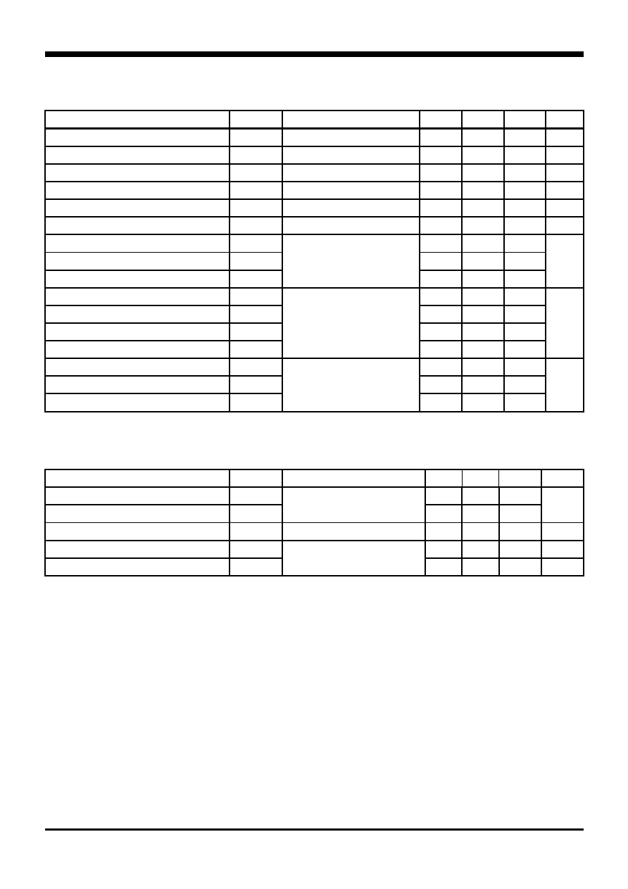
Absolute maximum ratings
(Tc=25
°C)
Characteristic Symbol
Rating
Unit
Drain-source voltage
V
DSS
600 V
Gate-source voltage
V
GSS
±30
V
(Tc=25)
1.0 A
Drain current (DC)
I
D
(Tc=100)
0.8 A
Drain current (Pulsed)
*
I
DP
4.0 A
Drain Power dissipation
P
D
18 W
Avalanche current (Single)
I
AS
1.0 A
Single pulsed avalanche energy
E
AS
22 mJ
Avalanche current (Repetitive)
I
AR
1.0 A
Repetitive avalanche energy
E
AR
2.5 mJ
Junction temperature
T
J
150
Storage temperature range
T
stg
-55~150
°C
* Limited by maximum junction temperature
Characteristic Symbol
Typ.
Max
Unit
Junction-case R
th(J-C)
-
6.94
Thermal
resistance
Junction-ambient R
th(J-a)
-
62.5
/W
KSD-T0O014-000
3
STK0160F
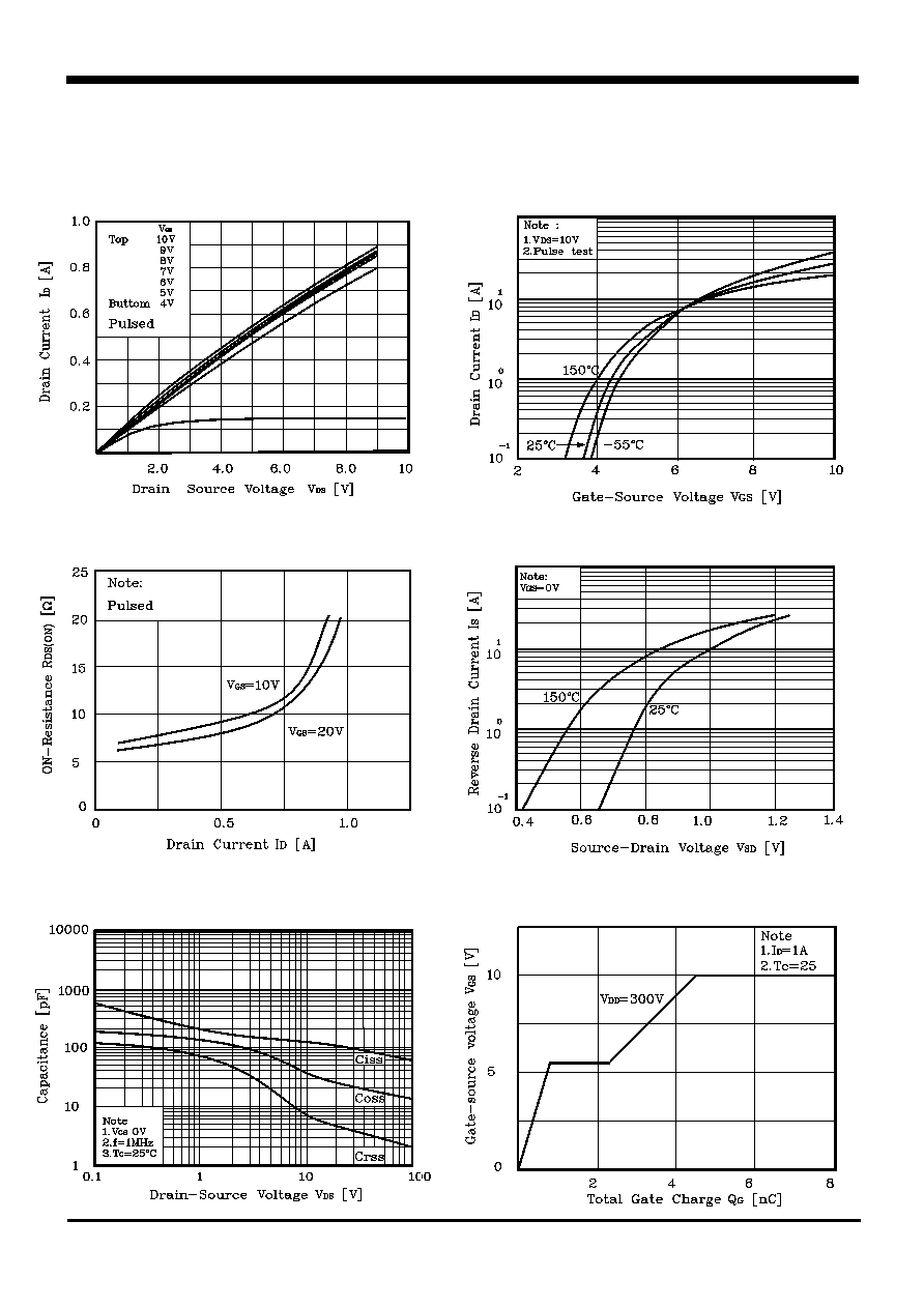
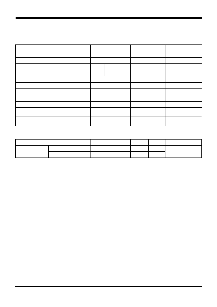
Electrical Characteristics
(Tc=25
°C)
Characteristic Symbol
Test
Condition
Min.
Typ.
Max.
Unit
Drain-source breakdown voltage
BV
DSS
I
D
=250µA, V
GS
=0
600 - - V
Gate-threshold voltage
V
GS(th)
I
D
=250µA, V
DS
= V
GS
2.0 - 4.0 V
Drain-source leakage current
I
DSS
V
DS
=600V, V
GS
=0V -
-
1
µA
Gate-source leakage
I
GSS
V
DS
=0V, V
GS
=±30V
- -
±100
nA
Drain-Source on-resistance
R
DS(ON)
V
GS
=10V, I
D
=0.5A -
8.8
9.4
Forward transfer admittance
g
fs
V
DS
=10V, I
D
=0.5A -
0.95
-
S
Input capacitance
Ciss -
150
225
Output capacitance
Coss
-
20
30
Reverse transfer capacitance
Crss
V
GS
=0V, V
DS
=25V, f=1MHz
- 4.3
6.4
pF
Turn-on delay time
t
d(on)
-
22.5
-
Rise time
t
r
-
27
-
Turn-off delay time
t
d(off)
-
11.5
-
Fall time
t
f
V
DD
=300V, V
GS
=10V
I
D
=1.0A, R
G
=25
- 27 -
ns
Total gate charge
Q
g
-
4.5
6.7
Gate-source charge
Q
gs
-
0.9
1.3
Gate-drain charge
Q
gd
V
DD
=300V, V
GS
=10V
I
D
=1.0A
- 1.3
1.9
nC
Source-Drain Diode Ratings and Characteristics
(Tc=25
°C)
Characteristic Symbol
Test
Condition
Min
Typ
Max
Unit
Continuous source current
I
S
-
-
1.0
Source current (Pulsed)
I
SM
Integral reverse diode
in the MOSFET
- - 4.0
A
Forward voltage
V
SD
V
GS
=0V, I
S
=1.0A -
-
1.4
V
Reverse recovery time
t
rr
-
160
-
ns
Reverse recovery charge
Q
rr
I
s
=1.0A, V
GS
=0V
di
s
/dt=100A/us
- 0.59 - uC
Note ;
Repetitive Rating : Pulse Width Limited by Maximum Junction Temperature
L=20mH, I
AS
=1.0A, V
DD
=50V, R
G
=25
Pulse Test : Pulse Width 300us, Duty cycle 2%
Essentially independent of operating temperature