KST-9016-000
1
STS9013
NPN Silicon Transistor
Descriptions
∑
General purpose application.
∑
Switching application.
Features
∑
Excellent h
FE
linearity.
∑
Complementary pair with STS9012
Ordering
Information
Type NO.
Marking
Package Code
STS9013
STS9013
TO-92
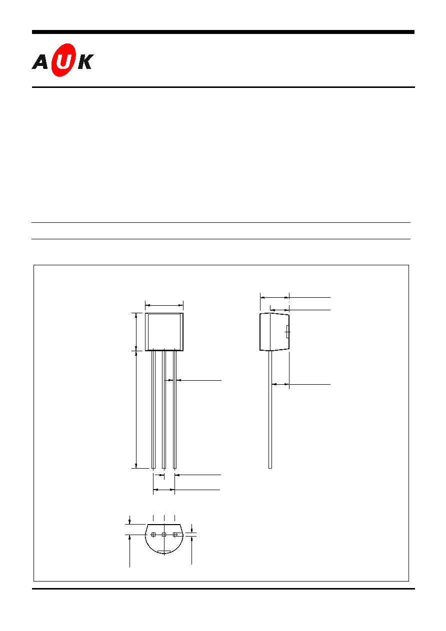
Outline Dimensions unit :
mm
S
S
e
e
m
m
i
i
c
c
o
o
n
n
d
d
u
u
c
c
t
t
o
o
r
r
4.5
±
0.1
4.
5
±
0.
1
0.4
±
0.02
1.27 Typ
.
2.54 Typ
.
1 2 3
3.45
±
0.1
2.25
±
0.1
2.06
±
0.1
1.
20
±
0.
1
0.
38
PIN Connections
1. Emitter
2. Base
3. Collector
14.
0
±
0.
40

KST-9016-000
2
STS9013
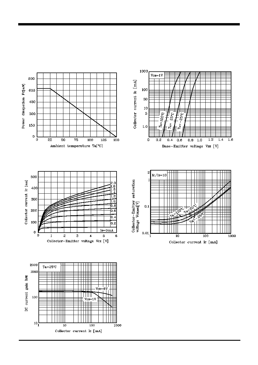
Absolute maximum ratings
(Ta=25
∞
∞
∞
∞
C)
Characteristic Symbol
Ratings
Unit
Collector-Base voltage
V
CBO
40 V
Collector-Emitter voltage
V
CEO
30 V
Emitter-Base voltage
V
EBO
5 V
Collector current
I
C
500
mA
Emitter current
I
E
-500
mA
Collector dissipation
P
C
625
mW
Junction temperature
T
j
150
∞
C
Storage temperature
T
stg
-55~150
∞
C
Electrical Characteristics
(Ta=25
∞
∞
∞
∞
C)
Characteristic
Symbol Test
Condition Min.
Typ.
Max.
Unit
Collector cut-off current
I
CBO
V
CB
=35, I
E
=0 -
-
0.1
µ
A
Emitter cut-off current
I
EBO
V
EB
=5V, I
C
=0 -
-
0.1
µ
A
DC current gain
h
FE
*
V
CE
=1V, I
C
=50mA 96
-
246
-
Collector-Emitter saturation voltage
V
CE(sat)
I
C
=100mA, I
B
=10mA -
0.1
0.25
V
Base-Emitter voltage
V
BE
I
C
=100mA, V
CE
=1V -
0.8
1
V
Transition frequency
f
T
V
CE
=6V, I
C
=20mA 140
-
-
MHz
Collector output capacitance
C
ob
V
CB
=6V, I
E
=0, f=1MHz
-
7.0
-
pF
* : h
FE
Rank / F : 96~135, G : 118~166, H : 144~202, I : 176~246.