 | ÐлекÑÑоннÑй компоненÑ: SW1314E-V | СкаÑаÑÑ:  PDF PDF  ZIP ZIP |
Äîêóìåíòàöèÿ è îïèñàíèÿ www.docs.chipfind.ru
KLW-3000-000
1
SW1314E-V
Chip LED Lamp
Features
· 1.6mm(L)×0.8mm small size surface mount type
· Thin package of 0.4mm(H) thickness
· Transparent clear lens optic
· Low power consumption type chip LED
· E ; ESD Protected (±2.0kv, 3 times @100pF, 1.5k)
Applications
· LCD backlighting
· Keypad backlighting
· Symbol backlighting
· Front panel indicator lamp
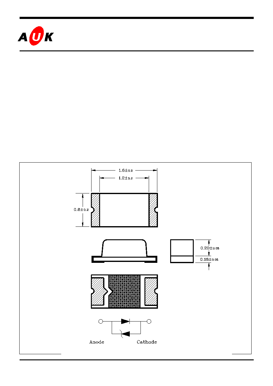
Outline Dimensions unit :
mm
S
S
e
e
m
m
i
i
c
c
o
o
n
n
d
d
u
u
c
c
t
t
o
o
r
r
KLW-3000-000
2
SW1314E-V
Absolute maximum ratings
Characteristic Symbol
Ratings
Unit
Power Dissipation
P
D
80
mW
Forward Current
I
F
20
mA
*
1
Peak Forward Current
I
FP
50
mA
Reverse Voltage
V
R
4
V
Operating Temperature
T
opr
-2580
Storage Temperature
T
stg
-30100
*
2
Soldering Temperature
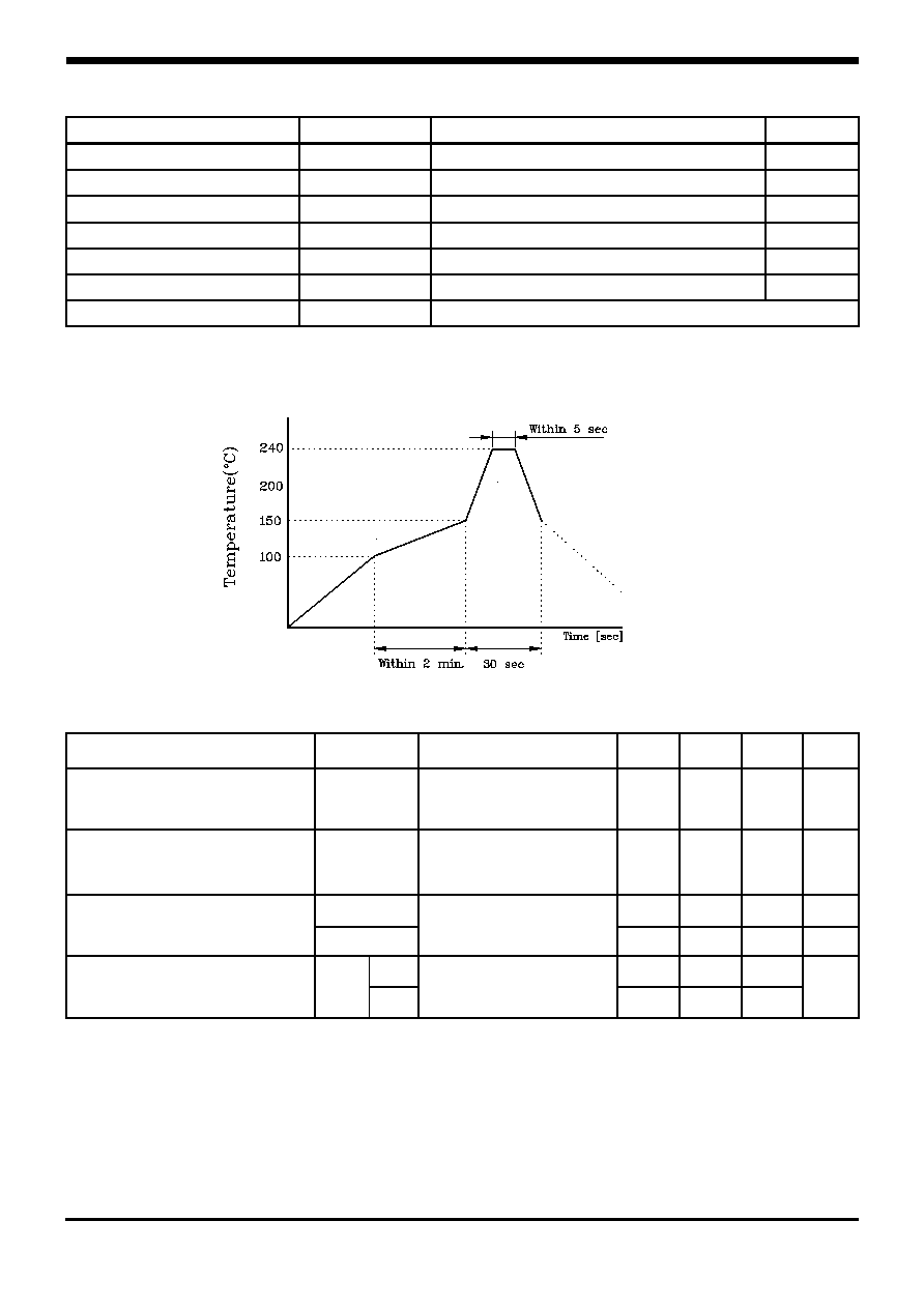
T
sol
240 for 5 seconds
*1.Duty ratio = 1/16, Pulse width = 0.1ms
*2. Recommended soldering Temperature Profile
2-1) Preheating 100 to 150 within 2 minutes Soldering 240 within 5 seconds
Gradual cooling (Avoid quenching)
Electrical Characteristics
Characteristic Symbol
Test
Condition
Min
Typ
Max
Unit
Forward Voltage
V
F
I
F
= 5mA
-
3.1
3.4
V
*
3
Luminous Intensity
I
V
I
F
= 5mA
15
40
65
mcd
X 0.160
-
0.230
-
*
4
Chromaticity Coordinates
Y
I
F
= 5mA
0.120 - 0.230 -
X
-
±65
-
*
5
Half Angle
1/2
Y
I
F
= 5mA
-
±70
-
deg
KLW-3000-000
3
SW1314E-V
*3. Forward Voltage Maximum tolerance for ±0.1V
*4. Luminous Intensity Maximum tolerance for each Grade Classification limit is ±18%
(The test result of IF=5mA is only for reference)
*5. CIE Coordinates bin limits will have ±0.02 tolerance
*6.
1/2
is the off-axis angle where the luminous intensity is
1/2
the peak intensity
Iv / VF Grade Classification
Test Condition @IF=5mA
Luminous Intensity
Forward Voltage
A : 13~22
0 : 2.6~2.8
B : 22~38
1 : 2.8~3.0
C : 38~65
2 : 3.0~3.2
3 : 3.2~3.4
(Do not use to combine grade classification. It must be used separately grade classification)
KLW-3000-000
4
SW1314E-V
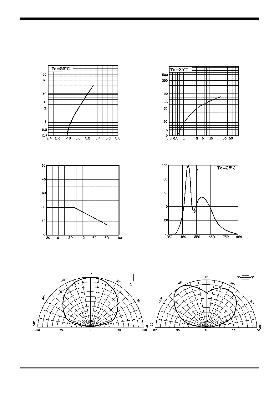
Characteristic Diagrams
Fig.4 Spectrum Distribution
Fig. 3 I
F
Ta
Fig. 2 I
V
- I
F
Fig. 1 I
F
- V
F
F
o
rward Current
I
F
[mA]
Ambient Temperature Ta []
R
e
lative Intensit
y
[%]
Wavelength [nm]
Forward Voltage V
F
[V]
F
o
rward Current
I
F
[mA]
Forward Current I
F
[mA]
Luminous Intensit
y I
v
[mcd]
Fig. 5-1 Radiation Diagram(X)
Relative Luminous Intensity Iv [%]
Fig. 5-2 Radiation Diagram(Y)
Relative Luminous Intensity Iv [%]
KLW-3000-000
5
SW1314E-V
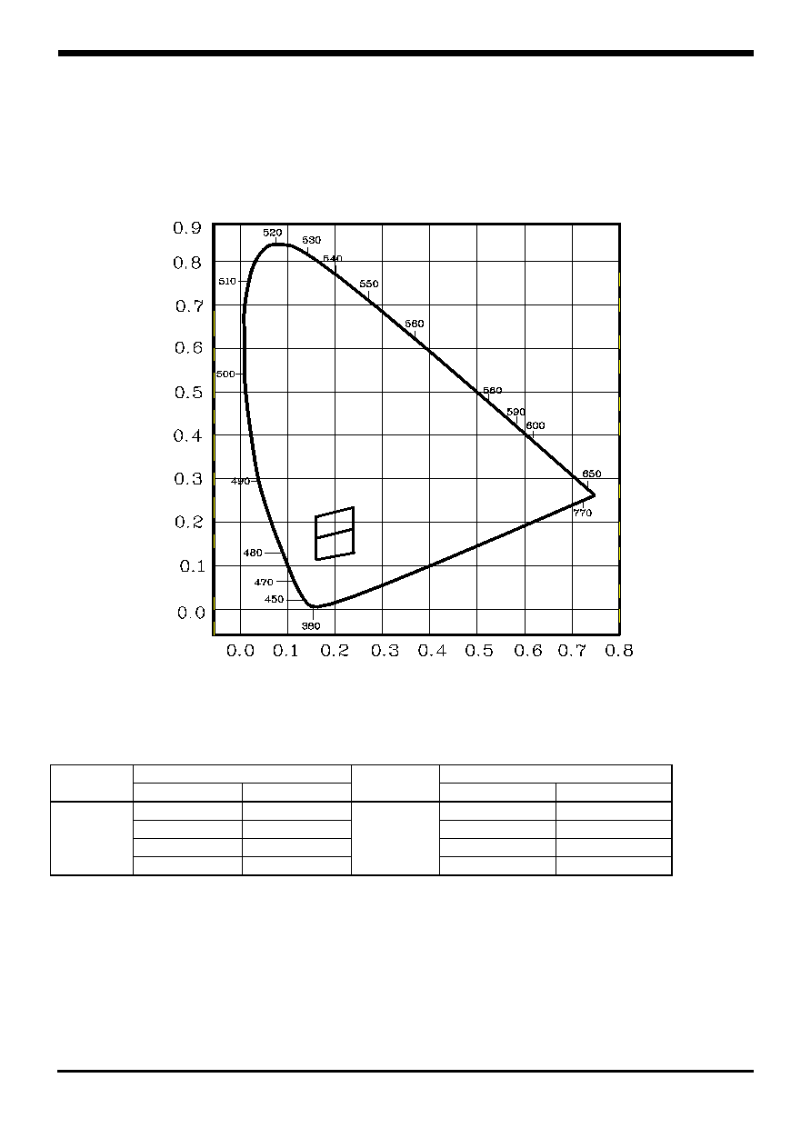
CIE Coordinates Grade Classification
CIE
Coordinates
CIE
Coordinates
Color Bin
X
Y
Color Bin
X
Y
0.160
0.210
0.160
0.165
0.160
0.165
0.160
0.120
0.230
0.185
0.230
0.140
a
0.230
0.230
b
0.230
0.185
CIE 1931 UCS Diagram
Chromaticity Diagr
a
m(Y)
Chromaticity Diagram(Y)
a
b