 | ÐлекÑÑоннÑй компоненÑ: SW3317E-G | СкаÑаÑÑ:  PDF PDF  ZIP ZIP |
Äîêóìåíòàöèÿ è îïèñàíèÿ www.docs.chipfind.ru
KSD-O2B033-000
1
SW3317E-G / SW3317E-G(B)
High Brightness White LED Lamp
2
1
2
1
2.80~3.20
2 . 7 0 ~ 3 . 1 0
5 . 1 0 ~ 5 . 5 0
2 3 . 0 0 M i n .
0 . 7 0 M a x .
1 . 0 0 M i n .
2 . 5 4 T y p .
3 . 5 0 ~ 3 . 9 0
3 . 6 0 ~ 4 . 0 0
0
.
4
5
M
a
x
.
2.80~3.20
2 . 7 0 ~ 3 . 1 0
5 . 1 0 ~ 5 . 5 0
4 . 7 0 ~ 5 . 7 0
2 3 . 0 0 M i n .
1 . 0 0 M i n .
2 . 5 4 T y p .
3 . 5 0 ~ 3 . 9 0
3 . 6 0 ~ 4 . 0 0
0
.
4
5
M
a
x
.
1 . 2 0 M i n .
0 . 7 0 M a x .
1
.
2
7
T
y
p
.
Features
· Colorless transparency lens type
· 3mm(T-1) all plastic mold type
· White emission color : X=0.17~0.29
Y=0.14~0.34
· E ; ESD Protected (±2.0KV, 3 Times @100pF, 1.5K)
· Viewing angle :
±
22
o
· Super luminosity
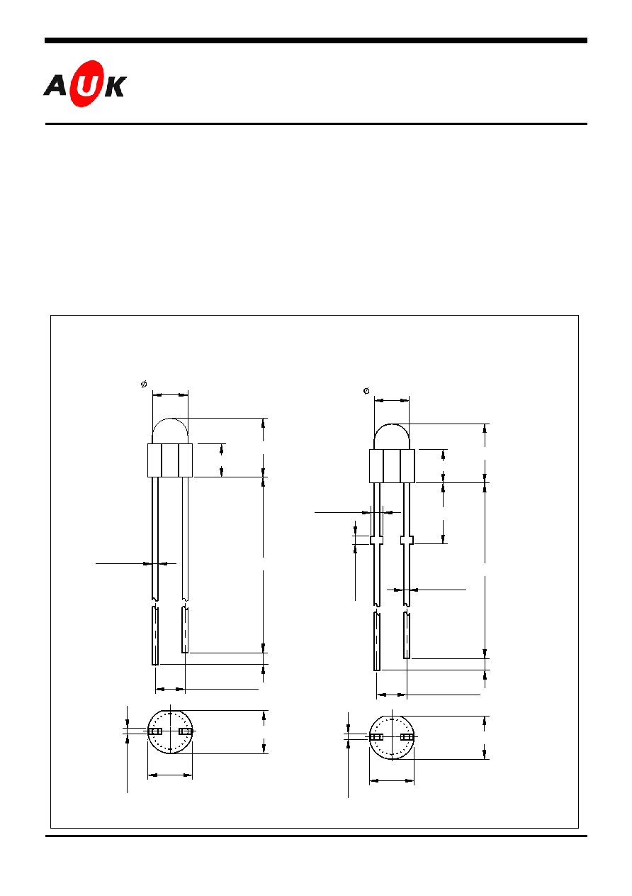
Outline Dimensions unit :
mm
S
S
e
e
m
m
i
i
c
c
o
o
n
n
d
d
u
u
c
c
t
t
o
o
r
r
STRAIGHT TYPE STOPPER TYPE : (B)
PIN Connections
1. Anode
2. Cathode
KSD-O2B033-000
2
SW3317E-G / SW3317E-G(B)
Absolute Maximum Ratings
(Ta=25
o
C)
Characteristic Symbol
Ratings
Unit
Power dissipation
P
D
110
mW
Forward current
I
F
30
mA
*
1
Peak forward current
I
FP
50
mA
Reverse voltage
V
R
4
V
Operating temperature range
T
opr
-25 85
Storage temperature range
T
stg
-30 100
*
2
Soldering temperature
T
sol
260 for
10
seconds
*1.Duty ratio = 1/16, Pulse width = 0.1ms
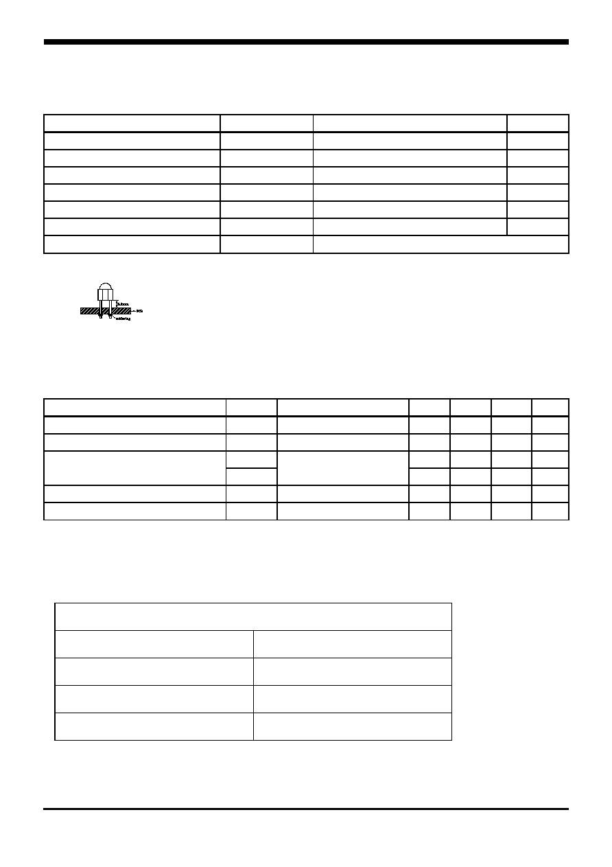
*2.Keep the distance more than 2.0mm from PCB to the bottom of LED package
Recommend document
-. LED is very sensitive to ESD.
Electrical / Optical Characteristics
(Ta=25
o
C)
Characteristic Symbol
Test
Condition
Min.
Typ.
Max.
Unit
Forward voltage
V
F
I
F
= 20mA
2.9
-
3.8
V
*
5
Luminous intensity
I
V
I
F
= 20mA
520
-
1760
mcd
X 0.17
-
0.29
-
*
3
Chromaticity coordinates
Y
I
F
= 20mA
0.14 - 0.34 -
Reverse current
I
R
V
R
=4V -
-
40
uA
*
4
Half angle
1/2
I
F
= 20mA
-
±22
- deg
*3. The chromaticity coordinates are derived from the CIE 1931 Chromaticity Diagram and represent
the perceived color of the device.
*4. 1/2 is the off-axis angle where the luminous intensity is 1/2 the peak intensity
*5. Luminous intensity maximum tolerance for each grade classification limit is ±18%
V
F
/ I
V
Grade Classification (Ta=25)
Test Condition @ I
F
=20mA
Forward Voltage [V]
Luminous Intensity [mcd]
1 : 2.9~3.2
P : 520~780
2 : 3.2~3.5
Q : 780~1170
3 : 3.5~3.8
R : 1170~1760
KSD-O2B033-000
3
SW3317E-G / SW3317E-G(B)
Characteristic Diagrams
Fig.4 Spectrum Distribution
Fig. 3 I
F
Ta
Fig. 2 I
V
- I
F
Fig. 1 I
F
- V
F
F
o
rward Current
I
F
[mA]
Ambient Temperature Ta []
R
e
lative Int
e
nsit
y
[%]
Wavelength [nm]
Forward Voltage V
F
[V]
F
o
rward Current
I
F
[mA]
Forward Current I
F
[mA]
Luminous Intensit
y I
v
[mc
d
]
Fig. 5 Radiation Diagram
100
50
50
0
100
Relative Luminous Intensity Iv [%]
KSD-O2B033-000
4
SW3317E-G / SW3317E-G(B)
CIE Coordinates Grade Classification (Ta=25, I
F
=20mA)
CIE Coordinates
CIE Coordinates
CIE Coordinates
Color
Bin
X Y
Color
Bin
X
X
Color
Bin
X Y
0.17 0.21
0.21 0.26
0.25 0.30
0.17 0.14
0.21 0.20
0.25 0.24
0.21 0.18
0.25 0.24
0.29 0.28
a
0.21 0.25
b
0.25 0.30
c
0.29 0.34
(Do not use to combine grade classification. It must be used separately grade classification)
CIE 1931 UCS Diagram
0.12
0.17
0.22
0.27
0.32
0.15
0.17
0.19
0.21
0.23
0.25
0.27
0.29
0.31
CIE Coordinate X
CI
E
Co
o
r
d
i
n
a
t
e
Y
0
0.1
0.2
0.3
0.4
0.5
0.6
0.7
0.8
0.9
0
0.1
0.2
0.3
0.4
0.5
0.6
0.7
0.8
CIE Coordinate X
CI
E
C
o
o
r
d
i
n
a
te
Y
490
600
540
550
480
470
450
380
580
590
830
510
520
530
500
495
630
a
c
b
KSD-O2B033-000
5
1. ESD(Electro Static Discharge) : Chip Al
2
o
3
(Sapphire: )
Chip Damage
V
F
Down
2. ESD
2-1. ESD (Electro Static Discharge) :
(+) (-)
( , , , )
(-) (+)
(+) (-) .
: , , , , ,
: , , , ,
: , .
2-2.
-.
.
80% .
-.
-. :
Wrist Strap ( ), Heel Grounder, , , ,
-. Conveyer Table
: Conductive Floor Mat
ESD
.
(10%~20%) (65%~90%)
Table
6[KV]
0.1[KV]
7[KV]
0.6[KV]
20[KV]
1.2[KV]