 | –≠–ª–µ–∫—Ç—Ä–æ–Ω–Ω—ã–π –∫–æ–º–ø–æ–Ω–µ–Ω—Ç: SW3318-GB | –°–∫–∞—á–∞—Ç—å:  PDF PDF  ZIP ZIP |
KLW-3001-000
1
SW3318-G / SW3318-G(B)
High Brightness LED Lamp
Features
∑ Colorless transparency lens type
∑ 3mm(T-1) all plastic mold type
∑ White emission color : X=0.22~0.36
Y=0.22~0.36
∑ Viewing angle : 22
o
∑ Super luminosity
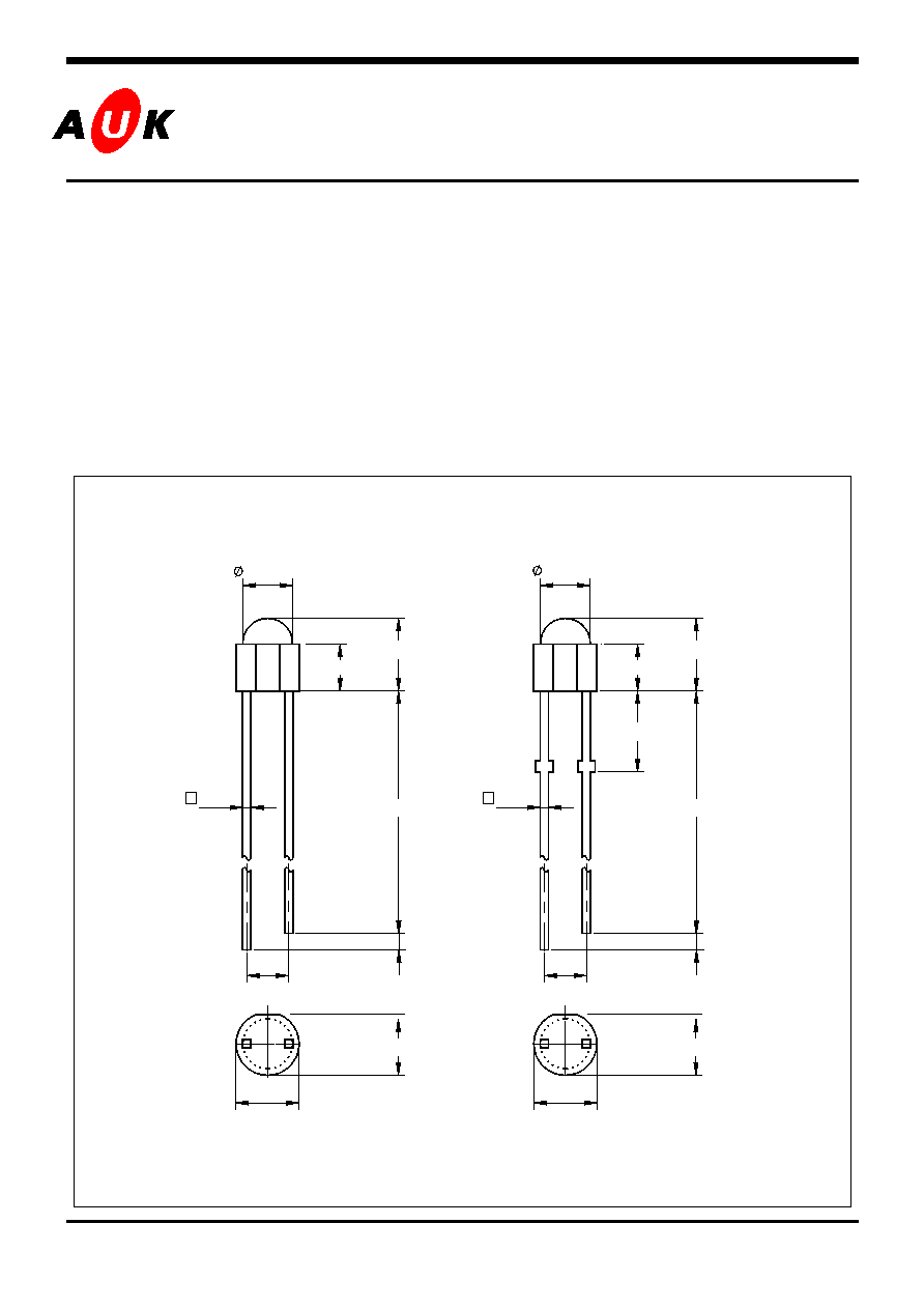
Outline Dimensions unit :
mm
S
S
e
e
m
m
i
i
c
c
o
o
n
n
d
d
u
u
c
c
t
t
o
o
r
r
STRAIGHT TYPE STOPPER TYPE
PIN Connections
1.Anode
2.Cathode
23.0 MIN
23.0 MIN
1
3.8±
0.2
2.54 NOM
3.8±
0.2
2
1
2.54 NOM
3.6±
0.2
1.0 MIN
3.6±
0.2
2
1.0 MIN
3.0±
0.2
4.1±
0.2
2.9±
0.2
0.4
0.4
3.0±
0.2
4.1±
0.2
5.5±
0.5
2.9±
0.2

KLW-3001-000
2
SW3318-G / SW3318-G(B)
Absolute maximum ratings
Characteristic Symbol
Ratings
Unit
Power Dissipation
P
D
85
mW
Forward Current
I
F
20
mA
*
1
Peak Forward Current
I
FP
50
mA
Reverse Voltage
V
R
4
V
Operating Temperature
T
opr
-2585
Storage Temperature
T
stg
-30100
*
2
Soldering Temperature
T
sol
260 for 5 seconds
*1.Duty ratio = 1/16, Pulse width = 0.1ms
*2.Keep the distance more than 2.0mm from PCB to the bottom of LED package
Recommend document
-. LED is very sensitive to ESD.
Electrical Characteristics
Characteristic Symbol
Test
Condition
Min.
Typ.
Max.
Unit
`` Forward Voltage
V
F
I
F
= 20mA
-
3.4
4.2
V
*
5
Luminous Intensity
I
V
I
F
= 20mA
-
500
-
mcd
X 0.21
-
0.29
-
*
3
Chromaticity Coordinates
Y
I
F
= 20mA
0.19 - 0.33 -
Reverse Current
I
R
V
R
=4V -
-
40
uA
*
4
Half angle
1/2
I
F
= 20mA
-
±45
- deg
*3. The chromaticity coordinates are derived from the CIE 1931 Chromaticity Diagram and represent
the perceived color of the device.
*4. 1/2 is the off-axis angle where the luminous intensity is 1/2 the peak intensity
*5. Luminous Intensity Maximum tolerance for each Grade Classification limit is ±18%
*5. Luminous Intensity classification
O
P
350~520 520~780
230~350
N
KLW-3001-000
3
SW3318-G / SW3318-G(B)
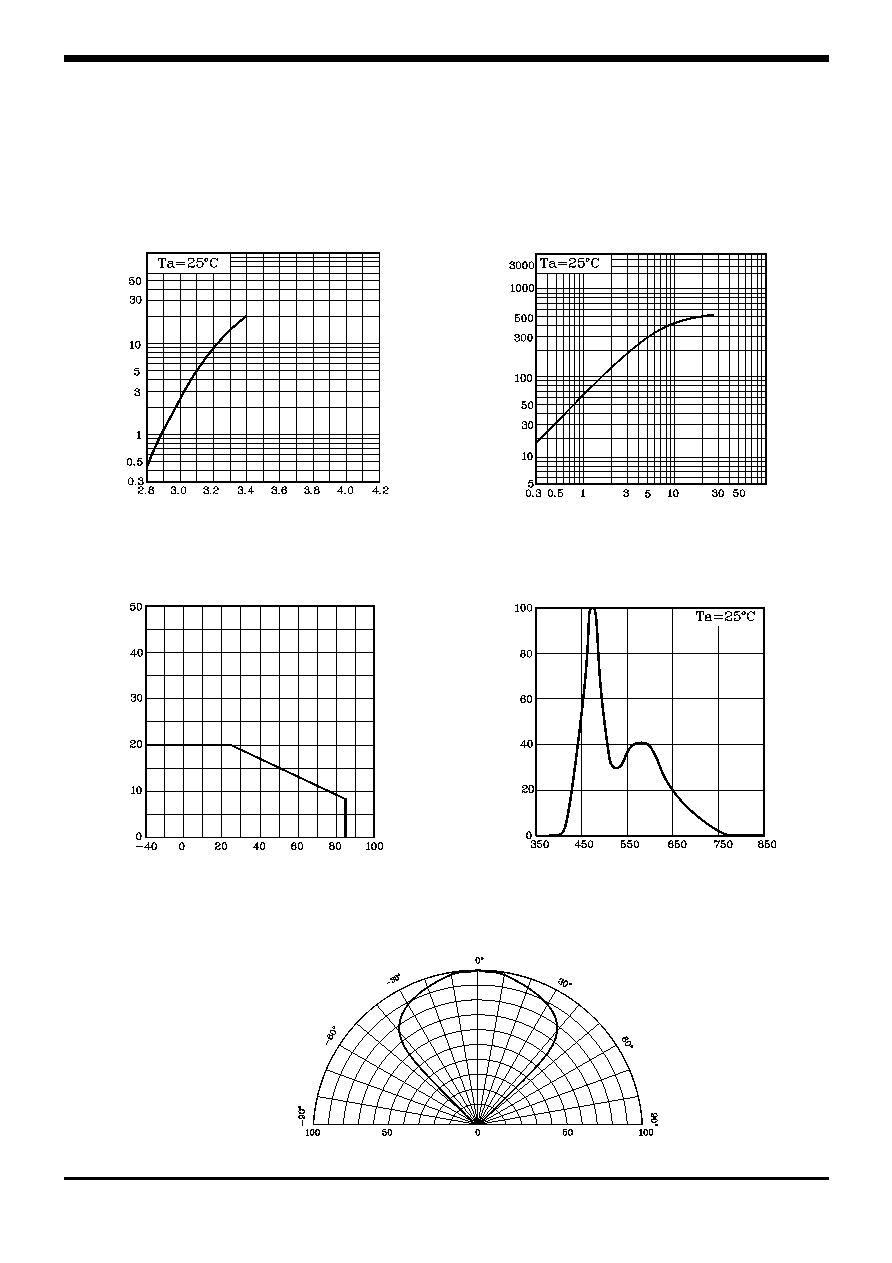
Characteristic Diagrams
Fig.4 Spectrum Distribution
Fig. 3 I
F
≠ Ta
Fig. 2 I
V
- I
F
Fig. 1 I
F
- V
F
F
o
rward Current
I
F
[mA]
Ambient Temperature Ta []
R
e
lative Intensit
y
[%]
Wavelength [nm]
Forward Voltage V
F
[V]
F
o
rward Current
I
F
[mA]
Forward Current I
F
[mA]
Luminous Intensit
y I
v
[mcd]
Fig. 5 Radiation Diagram
Relative Luminous Intensity Iv [%]

KLW-3001-000
4
1. ESD(Electro Static Discharge) : Chip Al
2
o
3
(Sapphire: )
Chip Damage
V
F
Down
2. ESD
2-1. ESD (Electro Static Discharge) :
(+) (-)
( , , , )
(-) (+)
(+) (-) .
: , , , , ,
: , , , ,
: , .
2-2.
-.
.
80% .
-.
-. :
Wrist Strap ( ), Heel Grounder, , , ,
-. Conveyer Table
: Conductive Floor Mat
ESD
.
(10%~20%) (65%~90%)
Table
6[KV]
0.1[KV]
7[KV]
0.6[KV]
20[KV]
1.2[KV]

KLW-3001-000
5
SW3318-G / SW3318-G(B)
These AUK products are intended for usage in general electronic equipments(Office and
communication equipment, measuring equipment, domestic electrification, etc.).
Please make sure that you consult with us before you use these AUK products in equipm-
ents which require high quality and/or reliability, and in equipments which could have
major impact to the welfare of human life(atomic energy control, airplane, spaceship, traffic
signal, combustion central, all types of safety device, etc.).
AUK cannot accept liability to any damage which may occur in case these AUK products
were used in the mentioned equipments without prior consultation with AUK.