SRAM
AS5C1008
Austin Semiconductor, Inc.
AS5C1008
Rev. 3.5 1/01
Austin Semiconductor, Inc. reserves the right to change products or specifications without notice.
1
FEATURES
∑ Access times of 15, 20 and 25 ns
∑ Fast output enable (t
AOE
) for cache applications
∑ Low active power
∑ Low standby power
∑ Fully static operation, no clock or refresh required
∑ TTL Compatible Inputs and Outputs
∑ Single +5V power supply
∑ Package in Industry-standard 32-pin SOJ
128K x 8 SRAM
RUGGEDIZED PLASTIC
HIGH SPEED SRAM
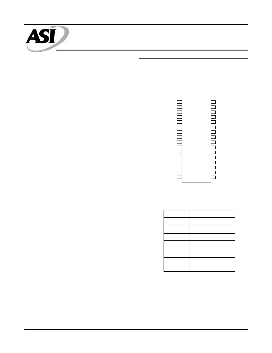
PIN ASSIGNMENT
(Top View)
32-Pin Plastic SOJ (DJ)
GENERAL DESCRIPTION
The ASI AS5C1008 is a high speed, low power, 128K by
8-bit ruggedized plastic (COTS) CMOS Static RAM. It is fabri-
cated using high performance, CMOS technology. This highly
reliable process coupled with innovative circuit design tech-
niques, yields access times as fast as 15ns (Max) over the
military and industrial temperature ranges.
When Chip Enable (CE\) is HIGH, the device assumes a
standby mode at which the power dissipation can be reduced
down to 125mW (max) at CMOS input levels.
Easy memory expansion is provided by using asserted LOW
CE\ and asserted HIGH CE2, and asserted LOW write enable
(
WE\) controls both writing and reading of the memory.
TheAS5C1008 is pin-compatible with other 128K x 8
SRAM's in the SOJ package.
*For ceramic versions of this product, please see the
MT5C1008 datasheet.
OPTIONS
MARKING
∑ Timing
15ns access
-15
20ns access
-20
25ns access
-25
∑ Package
Plastic SOJ*
DJ
No. 905
∑ Operating Temperature Ranges
-Military (-55
o
C to +125
o
C)
XT
-Industrial (-40
o
C to +85
o
C)
IT
For more products and information
please visit our web site at
www.austinsemiconductor.com
PIN FUNCTIONS
A0 - A16
Address Inputs
WE\
Write Enable
CE\
1
, CE
2
Chip Enable
OE\
Output Enable
I/O
0
- I/O
7
Data Inputs/Outputs
V
CC
Power
V
SS
Ground
NC
No Connection
1
2
3
4
5
6
7
8
9
1 0
1 1
1 2
1 3
1 4
1 5
1 6
NC
A6
A5
A4
A3
A2
A1
A0
A16
A15
A14
A13
I/O0
I/O1
I/02
Vss
3 2
3 1
3 0
2 9
2 8
2 7
2 6
2 5
2 4
2 3
2 2
2 1
2 0
1 9
1 8
1 7
Vcc
A7
CE
2
WE\
A8
A9
A10
A11
OE\
A12
CE\
1
I/O7
I/O6
I/O5
I/O4
I/O3
SRAM
AS5C1008
Austin Semiconductor, Inc.
AS5C1008
Rev. 3.5 1/01
Austin Semiconductor, Inc. reserves the right to change products or specifications without notice.
2
ABSOLUTE MAXIMUM RATINGS*
Vcc Supply Relative to GND...................................-0.5V to +7.0V
Voltage on any pin Relative to GND.........-0.5V to Vcc +7.0V
Storage Temperature ............................................-65
∞
C to +150
∞
C
Ambient Temperature with Power Applied........-55
o
C to +125
o
C
Short Circuit Output Current.................................................260
o
C
Power Dissipation...................................................................1.0W
*Stresses greater than those listed under "Absolute Maximum
Ratings" may cause permanent damage to the device. This is
a stress rating only and functional operation of the device at
these or any other conditions above those indicated in the
operation section of this specification is not implied. Exposure
to absolute maximum rating conditions for extended periods
may affect reliability.
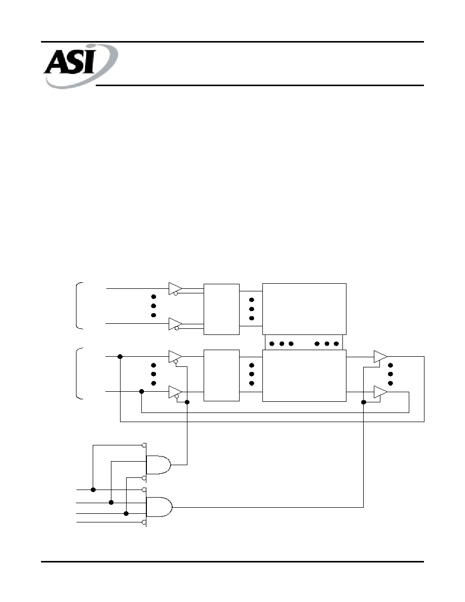
FUNCTIONAL BLOCK DIAGRAM
A0
Address
A16
I/O0
Data
I/O7
CE\
1
CE
2
WE\
OE\
Decoder
Input Data
Control
Memory Matrix
Column I/O
SRAM
AS5C1008
Austin Semiconductor, Inc.
AS5C1008
Rev. 3.5 1/01
Austin Semiconductor, Inc. reserves the right to change products or specifications without notice.
3
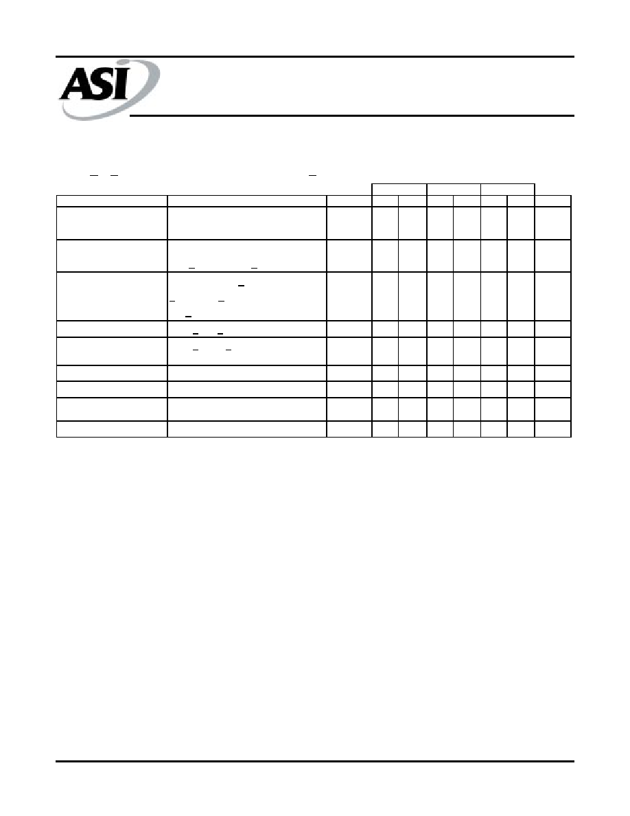
PARAMETER
CONDITIONS
SYMBOL MIN
MAX MIN MAX MIN MAX UNITS
Dynamic Operating
Current
Vcc=MAX, I
OUT
= 0mA,
CE
1
= V
IL
and CE
2
= V
IH
, f = fmax
I
CC1
180
150
140
mA
TTL Standby Current -
TTL Inputs
Vcc=MAX, V
IN
= V
IH
or V
IL
,
CE\
1
> V
IH
and CE
2
> V
IL
, f = fmax
I
SB1
90
75
70
mA
CMOS Standby Current -
CMOS Inputs
Vcc=MAX, CE\
1
> Vcc -0.2V, or CE
2
< 0.2V, V
IN
> Vcc -0.2V and
V
IN
< 0.2V, f = 0
I
SB2
10
10
10
mA
Input Leakage Current
GND < V
IN
< Vcc
I
LI
-10
10
-10
10
-10
10
µ
A
Output Leakage Current
GND < V
OUT
< Vcc
Output Disabled
I
LO
-10
10
-10
10
-10
10
µ
A
Output High Voltage
Vcc = MIN, I
OH
= -4.0 mA
V
OH
2.4
2.4
2.4
V
Output Low Voltage
Vcc = MIN, I
OL
= 8.0 mA
V
OL
0.4
0.4
0.4
V
Input High Voltage
V
IH
2.2
Vcc
+0.5
2.2
Vcc
+0.5
2.2
Vcc
+0.5
V
Input Low Voltage
V
IL
-0.5
0.8
-0.5
0.8
-0.5
0.8
V
-15
-20
-25
ELECTRICAL CHARACTERISTICS AND RECOMMENDED DC OPERATING CONDITIONS
(-55
o
C<T
A
<+125
o
C or -40
o
C to +85
o
C; Vcc = 5V+10%)
PIN DESCRIPTIONS
A0 - A16: Address Inputs
These 17 address inputs select one of the 131,072 8-bit words in
the RAM.
CE\
1
: Chip Enable 1 Input
CE\
1
is asserted LOW to read from or write to the device. If Chip
Enable 1 is deasserted, the device is deselected and is in standby
power mode. The I/O pins will be in the high-impedance state
when the device is deselected.
CE
2
: Chip Enable 2 Input
CE
2
is asserted HIGH to read from or write to the device. If Chip
Enable 2 is deasserted, the device is deselected and is in standby
power mode. The I/O pins will be in the high-impedance state
when the device is deselected.
OE\: Output Enable Input
The Output Enable Input is asserted LOW. If asserted LOW
while CE\
1
is asserted (LOW) and CE
2
is asserted (HIGH) and
WE\ is deasserted (HIGH), data from the SRAM will be present
on the I/O pins. The I/O pins will be in the high-impedance
state when OE\ is deasserted.
WE\: Write Enable Input
The Write Enable input is asserted LOW and controls read and
write operations. When CE\
1
and WE\ are both asserted (LOW)
and CE
2
is asserted (HIGH) input data present on the I/O pins
will be written into the selected memory location.
SRAM
AS5C1008
Austin Semiconductor, Inc.
AS5C1008
Rev. 3.5 1/01
Austin Semiconductor, Inc. reserves the right to change products or specifications without notice.
4
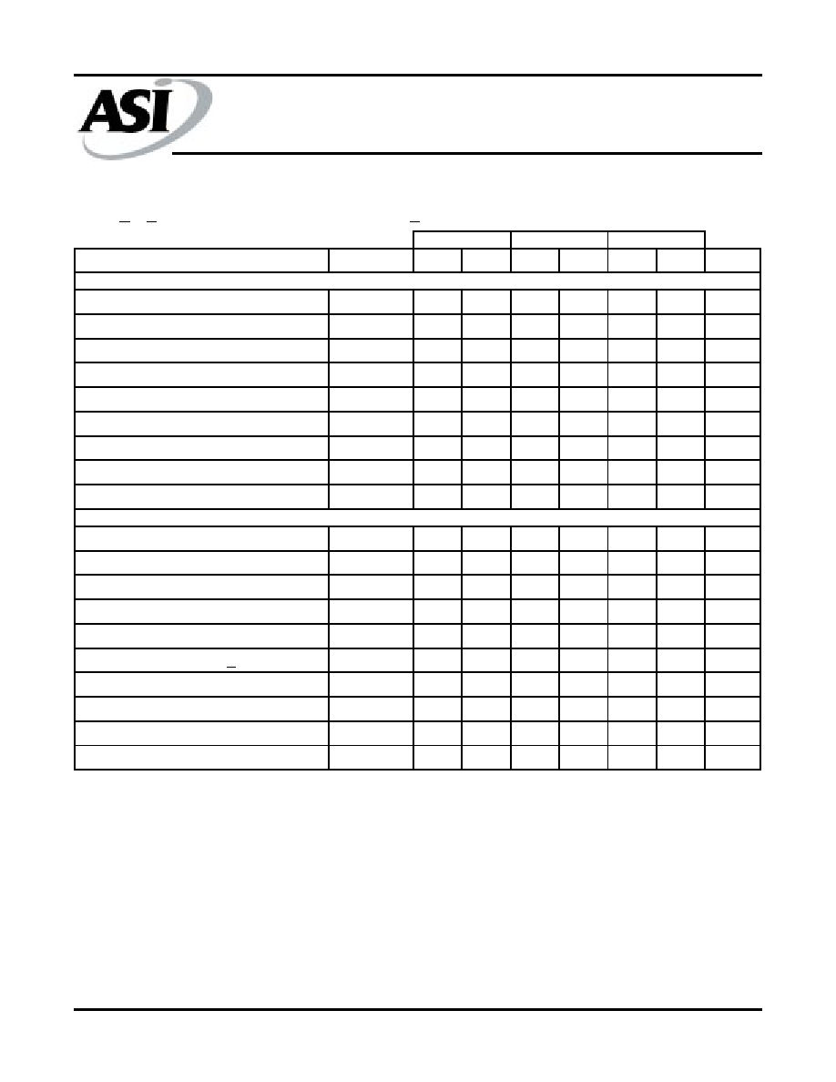
ELECTRICAL CHARACTERISTICS AND RECOMMENDED AC OPERATING CONDITIONS
(-55
o
C<T
A
<+125
o
C or -40
o
C to +85
o
C; Vcc = 5V+10%)
DESCRIPTION
SYMBOL
1
MIN
MAX
MIN
MAX
MIN
MAX
UNIT
READ CYCLE
Read Cycle Time
t
RC
15
20
25
ns
Address Access Time
t
AA
15
20
25
ns
Chip Enable Access Time
t
ACE
15
20
25
ns
Output Hold from Address Change
t
OH
3
3
3
ns
Chip Enable to Output in Low-Z
t
LZCE
3
3
3
ns
Chip Disable to Output in High-Z
t
HZCE
7
8
10
ns
Output Enable Access Time
t
AOE
7
7
10
ns
Output Enable to Output in Low-Z
t
LZOE
0
0
0
ns
Output Disable to Output in High-Z
t
HZOE
7
8
10
ns
WRITE CYCLE
Write Cycle Time
t
WC
15
20
25
ns
Chip Enable to End of Write
t
CW
12
15
20
ns
Address Valid to End of Write
t
AW
12
15
20
ns
Address Set-up Time
t
AS
0
0
0
ns
Address Hold from End of Write
t
AH
0
0
0
ns
Write Pulse Width (OE\ > V
IH
)
t
WP
12
15
20
ns
Data Set-up Time
t
DS
8
10
15
ns
Data Hold Time
t
DH
0
0
0
ns
Write Disable to Output in Low-Z
t
LZWE
5
5
5
ns
Write Enable to Output in High-Z
t
HZWE
7
9
10
ns
-15
-20
-25
NOTE: 1. t
LZCE
, t
LZWE
, t
HZCE
, t
LZOE
, and t
HZOE
are simulated values.

SRAM
AS5C1008
Austin Semiconductor, Inc.
AS5C1008
Rev. 3.5 1/01
Austin Semiconductor, Inc. reserves the right to change products or specifications without notice.
5
Input Pulse Levels.......................................................GND to 3.0V
Input Rise and Fall Times..........................................................3ns
Input Timing Reference Levels................................................1.5V
Output Reference Levels..........................................................1.5V
Output Load..................................................................See Figure 1
AC TEST CONDITIONS
Fig. 1 OUTPUT LOAD EQUIVALENT
+5V
Q
255
30 pF
480
+5V
Q
255
5 pF
480
for t
LZCE
, t
HZCE
, t
LZWE
, t
HZWE
, t
LZOE
, and t
HZOE
CAPACITANCE (T
A
= +25
o
C, f = 1.0 MHz)
PARAMETER
CONDITION
SYMBOL
MAX
UNIT
Input Capacitance
V
IN
= 0V
C
IN
6
pF
Output Capacitance
V
OUT
= 0V
C
OUT
8
pF