SRAM
AS5C4008
Austin Semiconductor, Inc.
AS5C4008
Rev. 5.5 12/01
Austin Semiconductor, Inc. reserves the right to change products or specifications without notice.
1
AVAILABLE AS MILITARY
SPECIFICATION
∑ SMD 5962-95600
∑ SMD 5962-95613
∑ MIL STD-883
OPTIONS
MARKING
∑ Timing
15ns access (contact factory)
-15
17ns access
-17
20ns access
-20
25ns access
-25
35ns access
-35
45ns access
-45
∑ Operating Temperature Range
Military: -55
o
C to +125
o
C
XT
Industrial: -40
o
C to +85
o
C
IT
∑ Packages
Ceramic Dip (600 mil)
CW
No. 112
Ceramic Flatpack
F
No. 304
Ceramic LCC
EC
No. 209
Ceramic SOJ
ECJ
No. 502
Ceramic LCC (contact factory)
ECA
No. 208
∑ Options
2V data retention/ low power
L
NOTE: Not all combinations of operating temperature, speed, data retention and low
power are necessarily available. Please contact factory for availability of specific part
number combinations.
GENERAL DESCRIPTION
The AS5C4008 is a 4 megabit monolithic CMOS SRAM,
organized as a 512K x 8.
The evolutionary 32 pin device allows for easy upgrades from
the 1 meg SRAM.
For flexibility in high-speed memory applications, ASI offers
chip enable (CE\) and output enable (OE\) capabilities. These
enhancements can place the outputs in High-Z for additional flexibil-
ity in system design.
Writing to these devices is accomplished when write enable (WE\)
and CE\ inputs are both LOW. Reading is accomplished when WE\
remains HIGH and CE\ and OE\ go LOW. This allows systems
designers to meet low standby power requirements.
All devices operate from a single +5V power supply and all
inputs are fully TTL-Compatible.
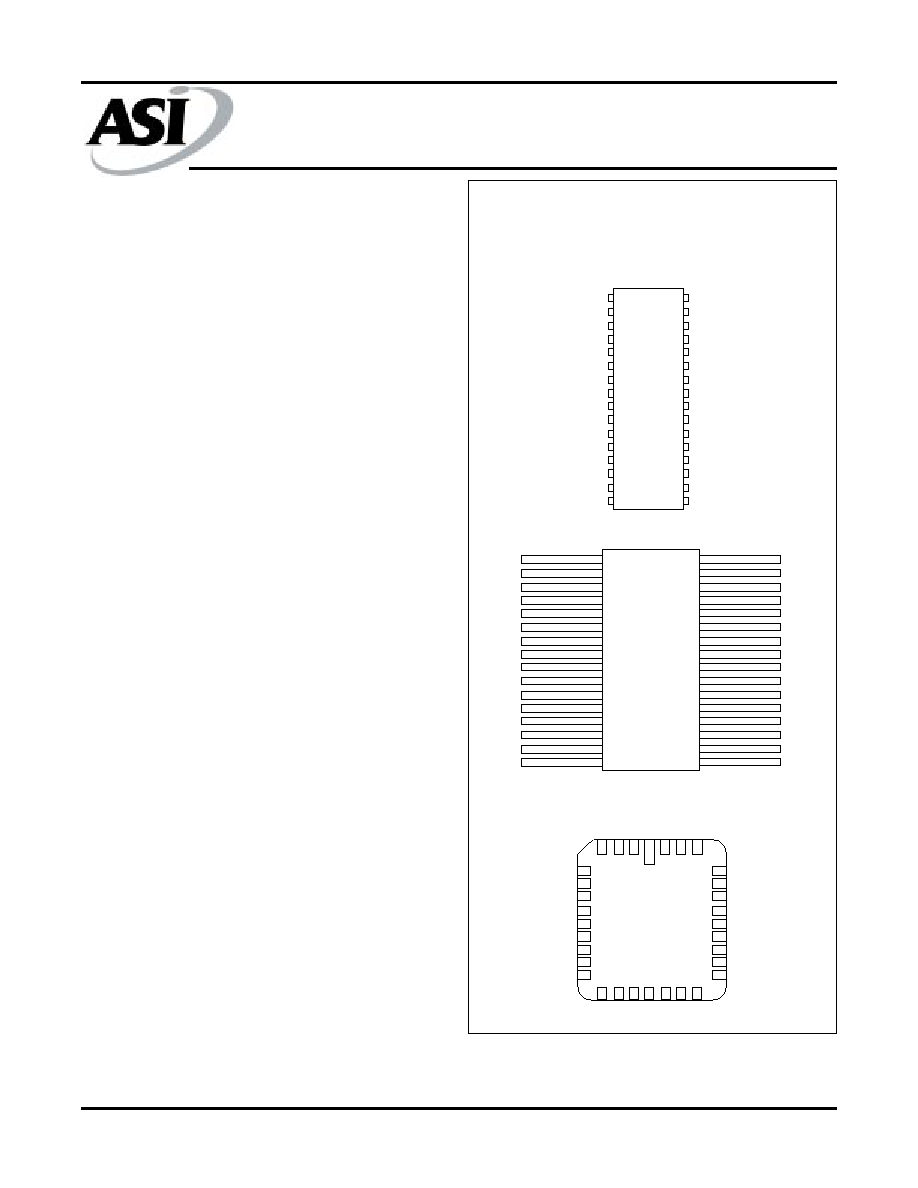
PIN ASSIGNMENT
(Top View)
32-Pin DIP (CW), 32-Pin LCC (EC)
32-Pin SOJ (ECJ)
512K x 8 SRAM
SRAM MEMORY ARRAY
For more products and information
please visit our web site at
www.austinsemiconductor.com
FEATURES
∑ High Speed: 17, 20, 25, 35 and 45ns
∑ High-performance, low power military grade device
∑ Single +5V ±10% power supply
∑ Easy memory expansion with CE\ and OE\ options
∑ All inputs and outputs are TTL-compatible
∑ Ease of upgradability from 1 Meg using the 32 pin
evolutionary version.
32-Pin Flat Pack (F)
32-Pin LCC (ECA)
A18
A16
A14
A12
A7
A6
A5
A4
A3
A2
A1
A0
I/O0
I/O1
I/O2
Vss
1
2
3
4
5
6
7
8
9
10
11
12
13
14
15
16
32
31
30
29
28
27
26
25
24
23
22
21
20
19
18
17
Vcc
A15
A17
WE\
A13
A8
A9
A11
OE\
A10
CE\
I/O7
I/O6
I/O5
I/O4
I/O3
A18
A16
A14
A12
A7
A6
A5
A4
A3
A2
A1
A0
I/O0
I/O1
I/O2
Vss
1
2
3
4
5
6
7
8
9
10
11
12
13
14
15
16
32
31
30
29
28
27
26
25
24
23
22
21
20
19
18
17
Vcc
A15
A17
WE\
A13
A8
A9
A11
OE\
A10
CE\
I/O7
I/O6
I/O5
I/O4
I/O3
A12
A14
A16
A18
Vcc
A15
A17
4 3 2 32 31 30
14 15 16 17 18 19 20
5
6
7
8
9
1 0
1 1
1 2
1 3
2 9
2 8
2 7
2 6
2 5
2 4
2 3
2 2
2 1
A7
A6
A5
A4
A3
A2
A1
A0
I/O0
WE\
A13
A8
A9
A11
OE\
A10
CE\
I/O 7
I/O6
I/O5
I/O4
I/O3
Vss
I/O2
I/O1
1

SRAM
AS5C4008
Austin Semiconductor, Inc.
AS5C4008
Rev. 5.5 12/01
Austin Semiconductor, Inc. reserves the right to change products or specifications without notice.
2
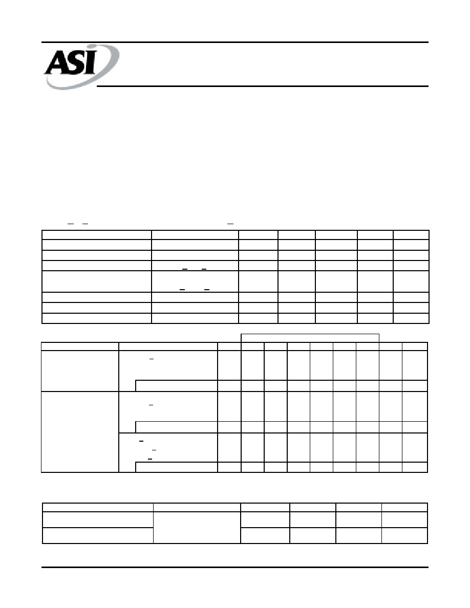
FUNCTIONAL BLOCK DIAGRAM
MODE
OE\
CE\
WE\
DQ
POWER
STANDBY
X
H
X
High-Z
STANDBY
READ
L
L
H
Q
ACTIVE
NOT SELECTED
H
L
H
High-Z
ACTIVE
WRITE
X
L
L
D
ACTIVE
TRUTH TABLE
Vcc
GND
I/O7
A0:A18
I/O1
CE\
OE\
WE\
Input Buffer
Row Decoder
2,097,152 Bit
Memory Array
I/O Control
Column Decoder
Power
Down
SRAM
AS5C4008
Austin Semiconductor, Inc.
AS5C4008
Rev. 5.5 12/01
Austin Semiconductor, Inc. reserves the right to change products or specifications without notice.
3
ABSOLUTE MAXIMUM RATINGS*
Voltage on Vcc Supply Relative to Vss...................-.5V to +7.0V
Storage Temperature ............................................-65
∞
C to +150
∞
C
Short Circuit Output Current (per I/O)................................20mA
Voltage on any Pin Relative to Vss......................-.5V to Vcc+1 V
Maximum Junction Temperature**....................................+150
∞
C
*Stresses greater than those listed under "Absolute
Maximum Ratings" may cause permanent damage to the
device. This is a stress rating only and functional opera-
tion of the device at these or any other conditions above
those indicated in the operation section of this specifica-
tion is not implied. Exposure to absolute maximum rating
conditions for extended periods may affect reliability.
** Junction temperature depends upon package type,
cycle time, loading, ambient temperature and airflow.
ELECTRICAL CHARACTERISTICS AND RECOMMENDED DC OPERATING CONDITIONS
(-55
o
C<T
A
<125
o
C or -40
o
C to +85
o
C; Vcc = 5V +10%)
CAPACITANCE
PARAMETER
CONDITION
SYMBOL
MIN
MAX
UNITS
NOTES
Input High (Logic 1) Voltage
V
IH
2.2
V
CC
+0.5
V
1
Input Low (Logic 0) Voltage
V
IL
-0.5
0.8
V
1, 2
Input Leakage Current
OV < V
IN
< Vcc
IL
I
-10
10
µ
Output Leakage Current
Output(s) disabled
OV < V
OUT
< Vcc
IL
O
-10
10
µ
Output High Voltage
I
OH
= -4.0 mA
V
OH
2.4
--
V
1
Output Low Voltage
I
OL
= 8.0 mA
V
OL
---
0.4
V
1
Supply Voltage
Vcc
4.5
5.5
V
1
SYM
-15
-17
-20
-25
-35
-45
UNITS NOTES
I
CCSP
225
225
225
225
225
225
mA
3
L Version Only
I
CCLP
180
180
180
180
180
180
mA
I
SBTSP
60
60
60
60
60
60
mA
L Version Only
I
SBTLP
30
30
30
30
30
30
mA
I
SBCSP
25
25
25
25
25
25
mA
L Version Only
I
SBCLP
10
10
10
10
10
10
mA
Power Supply Current:
Standby
PARAMETER
MAX
CE\ > V
IH
; Vcc = MAX
f = 0, Outputs Open
CE\ < V
IL
; Vcc = MAX
f = MAX = 1/t
RC
Outputs Open
CE\ < V
CC
-0.2V; Vcc = MAX
V
IN
< Vss +0.2V or
V
IN
> Vcc -0.2V; f = 0
CONDITIONS
Power Supply Current:
Operating
PARAMETER
CONDITIONS
SYMBOL
MAX
UNITS
NOTES
Input Capacitance
C
I
12
pF
4
Output Capactiance
Co
14
pF
4
T
A
= 25
o
C, f = 1MHz
V
IN
= 0
SRAM
AS5C4008
Austin Semiconductor, Inc.
AS5C4008
Rev. 5.5 12/01
Austin Semiconductor, Inc. reserves the right to change products or specifications without notice.
4
ELECTRICAL CHARACTERISTICS AND RECOMMENDED AC OPERATING CONDITIONS
(-55
o
C<T
A
<125
o
C or -40
o
C to +85
o
C; Vcc = 5V +10%)
�
�
�
�
! � "
# $%&
)
"%&
*
*
' ('
�
*
*
# $%&
�
�
�
�
�
�
)
"%&
*
*
' ('
�
+,
�
- +
(
.
- +
(
/
�
! � - +
+,
0 +
(
)
/
�
�
1
)
�
�
+
)
# $%&
�
�
�
�
�
�
+
"%&
*
*
' ('
SRAM
AS5C4008
Austin Semiconductor, Inc.
AS5C4008
Rev. 5.5 12/01
Austin Semiconductor, Inc. reserves the right to change products or specifications without notice.
5
NOTES
1.
All voltages referenced to V
SS
(GND).
2.
-2V for pulse width < 20ns
3.
I
CC
is dependent on output loading and cycle rates.
4.
This parameter is guaranteed but not tested.
5.
Test conditions as specified with the output loading
as shown in Fig. 1 unless otherwise noted.
6.
t
LZCE,
t
LZWE,
t
LZOE,
t
HZCE,
t
HZOE and
t
HZWE
are specified with CL = 5pF as in Fig. 2. Transition is
measured ±200mV from steady state voltage.
7.
At any given temperature and voltage condition,
t
HZCE is less than
t
LZCE, and
t
HZWE is less than
t
LZWE.
8.
WE\ is HIGH for READ cycle.
9.
Device is continuously selected. Chip enables and
output enables are held in their active state.
10. Address valid prior to, or coincident with, latest
occurring chip enable.
11.
t
RC = Read Cycle Time.
12. Chip enable and write enable can initiate and
terminate a WRITE cycle.
13. Output enable (OE\) is inactive (HIGH).
14. Output enable (OE\) is active (LOW).
15. ASI does not warrant functionality nor reliability of any
product in which the junction temperature exceeds
150∞C. Care should be taken to limit power to acceptable
levels.
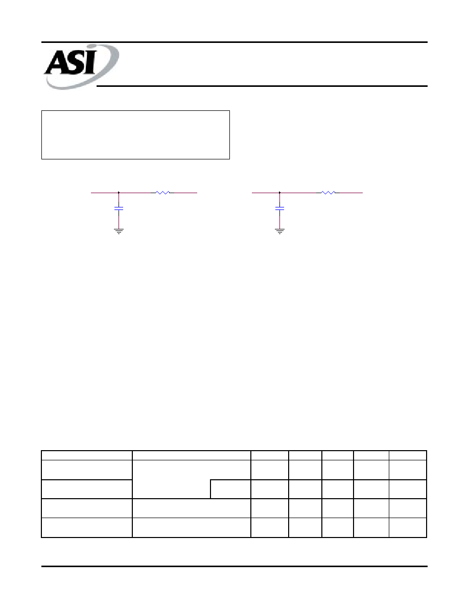
Fig. 1 Output Load Equivalent
Fig. 2 Output Load Equivalent
167 ohms
167 ohms
1.73V
1.73V
C=5pF
C=30pF
Q
Q
DATA RETENTION ELECTRICAL CHARACTERISTICS (L Version Only)
AC TEST CONDITIONS
Input pulse levels ................................................... Vss to 3.0V
Input rise and fall times ....................................................... 3ns
Input timing reference levels ............................................ 1.5V
Output reference levels ..................................................... 1.5V
Output load ............................................... See Figures 1 and 2
DESCRIPTION
SYMBOL
MIN
MAX
UNITS
NOTES
V
CC
for Retention Data
V
DR
2
V
Data Retention Current
(L Version Only)
V
CC
= 2V
I
CCDR
4.5
mA
Chip Deselect to Data
Retention Time
t
CDR
0
ns
4
Operation Recovery Time
t
R
10
ms
4, 11
CE\ > (Vcc -0.2V)
VIN > (Vcc -0.2V) or < 0.2V
CONDITIONS