
SRAM
AS5SS128K36
Austin Semiconductor, Inc.
AS5SS128K36
Rev. 2.0 12/00
Austin Semiconductor, Inc. reserves the right to change products or specifications without notice.
1
128K x 36 SSRAM
SYNCHRONOUS ZBL SRAM
FLOW-THRU OUTPUT
FEATURES
∑ High frequency and 100% bus utilization
∑ Fast cycle times: 11ns & 12ns
∑ Single +3.3V +5% power supply (V
DD
)
∑ Advanced control logic for minimum control signal interface
∑ Individual BYTE WRITE controls may be tied LOW
∑ Single R/W\ (READ/WRITE) control pin
∑ CKE\ pin to enable clock and suspend operations
∑ Three chip enables for simple depth expansion
∑ Clock-controlled and registered addresses, data I/Os and
control signals
∑ Internally self-timed, fully coherent WRITE
∑ Internally self-timed, registered outputs to eliminate the
need to control OE\
∑ SNOOZE MODE for reduced-power standby
∑ Common data inputs and data outputs
∑ Linear or Interleaved Burst Modes
∑ Burst feature (optional)
∑ Pin/function compatibility with 2Mb, 8Mb, and 16Mb ZBL
SRAM
∑ Automatic power-down
OPTIONS
MARKING
∑ Timing (Access/Cycle/MHz)
8.5ns/11ns/90 MHz
-11
9ns/12ns/83 MHz
-12
∑ Packages
100-pin TQFP
DQ No. 1001
∑ Operating Temperature Ranges
Military (-55
o
C to +125
o
C)
XT
Industrial (-40
o
C to +85
o
C)
IT
GENERAL DESCRIPTION
The Austin Semiconductor, Inc. Zero Bus Latency SRAM
family employs high-speed, low-power CMOS designs using an ad-
vanced CMOS process.
ASI's 4Mb ZBL SRAMs integrate a 128K x 36 SRAM core
with advanced synchronous peripheral circuitry and a 2-bit burst
counter. These SRAMS are optimized for 100 percent bus utilization,
eliminating any turnaround cycles for READ to WRITE, or WRITE
to READ, transitions. All synchronous inputs pass through registers
controlled by a positive-edge-triggered single clock input (CLK). The
synchronous inputs include all addresses, all data inputs, chip enable
(CE\), two additional chip enables for easy depth expansion (CE2,
CE2\), cycle start input (ADV/LD\), synchronous clock enable (CKE\),
byte write enables (BWa\, BWb\, BWc\, and BWd\) and read/write (R/
W\).
Asynchronous inputs include the output enable (OE\, which
may be tied LOW for control signal minimization), clock (CLK) and
snooze enable (ZZ, which may be tied LOW if unused). There is also
a burst mode pin (MODE) that selects between interleaved and linear
burst modes. MODE may be tied HIGH, LOW or left unconnected if
burst is unused. The flow-through data-out (Q) is enabled by OE\.
WRITE cycles can be from one to four bytes wide as controlled by the
write control inputs.
All READ, WRITE and DESELECT cycles are initiated by
the ADV/LD\ input. Subsequent burst addresses can be internally
generated as controlled by the burst advance pin (ADV/LD\). Use of
burst mode is optional. It is allowable to give an address for each
individual READ and WRITE cycle. BURST cycles wrap around
after the fourth access from a base address.
To allow for continuous, 100 percent use of the data bus,
the flow-through ZBL SRAM uses a LATE WRITE cycle. For ex-
ample, if a WRITE cycle begins in clock cycle one, the address is
present on rising edge one. BYTE WRITEs need to be asserted on the
same cycle as the address. The write data associated with the address
is required one cycle later, or on the rising edge of clock cycle two.
Address and write control are registered on-chip to simplify
WRITE cycles. This allows self-timed WRITE cycles. Individual
byte enables allow individual bytes to be written. During a BYTE
WRITE cycle, BWa\ controls DQa pins; BWb\ controls DQb pins;
BWc\ controls DQc pins; and BWd\ controls DQd pins. Cycle types
can only be defined when an address is loaded, i.e., when ADV/LD\ is
LOW. Parity/ECC bits are available on this device.
Austin's 4Mb ZBL SRAMs operate from a +3.3V V
DD
power supply, and all inputs and outputs are LVTTL-compatible.
The device is ideally suited for systems requiring high bandwidth and
zero bus turnaround delays.
For more products and information
please visit our web site at
www.austinsemiconductor.com
SRAM
AS5SS128K36
Austin Semiconductor, Inc.
AS5SS128K36
Rev. 2.0 12/00
Austin Semiconductor, Inc. reserves the right to change products or specifications without notice.
2
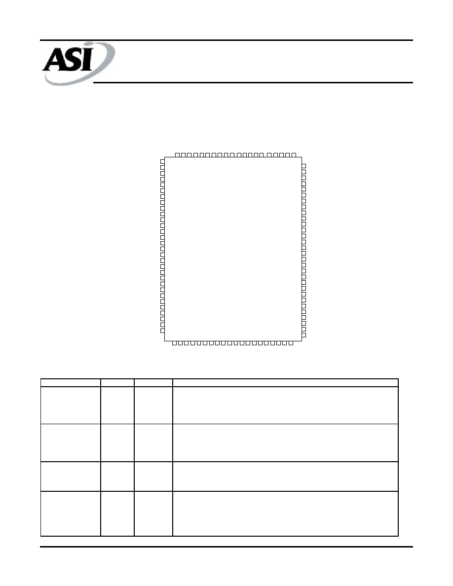
PIN ASSIGNMENT
(Top View)
100-pin TQFP (DQ)
PIN DESCRIPTIONS
TQFP PINS
SYMBOL
TYPE
DESCRIPTION
37
36
32-35, 44-50,
81, 82, 99, 100
SA0
SA1
SA
Input
Synchronous Address Inputs: These inputs are registered and must meet the setup
and hold times around the rising edge of CLK. Pins 83 and 84 are reserved as
address bits for the higher-density 8Mb and 16Mb ZBL SRAMs, respectively. SA0 and
SA1 are the two least significant bits (LSB) of the address field and set the internal
burst counter if burst is desired.
93
94
95
96
BWa\
BWb\
BWc\
BWd\
Input
Synchronous Byte Write Enables:
These active LOW inputs allow individual bytes to
be written when a WRITE cycle is active and must meet the setup and hold times
around the rising edge of CLK.
BYTE WRITEs need to be asserted on the same cycle
as the address.
BWa\ controls DQa pins; BWb\ controls DQb pins; BWc\ controls
DQc pins; BWd\ controls DQd pins.
87
CKE\
Input
Synchronous
Clock
Enable:
This
active
LOW
input
permits
CLK
to
propagate
throughout the device.
When CKE is HIGH, the device ignores the CLK input and
effectively internally extends the previous CLK cycle.
This input must meet setup and
hold times around the rising edge of CLK.
88
R/W\
Input
Read/Write:
This input determines the cycle type when ADV/LD\ is LOW and is the
only means for determining READs and WRITEs.
READ cycles may not be converted
into WRITEs (and vice versa) other than by loading a new address.
A LOW on this pin
permits BYTE WRITE operations and must meet the setup and hold times around the
rising edge of CLK. Full bus-width WRITEs occur if all byte write enables are LOW.
1
2
3
4
5
6
7
8
9
10
11
12
13
14
15
16
17
18
19
20
21
22
23
24
25
26
27
28
29
30
80
79
78
77
76
75
74
73
72
71
70
69
68
67
66
65
64
63
62
61
60
59
58
57
56
55
54
53
52
51
31 32 33 34 35 36 37 38 39 40 41 42 43 44 45 46 47 48 49 50
100 99 98 97 96 95 94 93 92 91 90 89 88 87 86 85 84 83 82 81
DQc
DQc
DQc
V
DD
Q
V
SS
DQc
DQc
DQc
DQc
V
SS
V
DD
Q
DQc
DQc
V
SS
V
DD
V
DD
V
SS
DQd
DQd
V
DD
Q
V
SS
DQd
DQd
DQd
DQd
V
SS
V
DD
Q
DQd
DQd
DQd
DQb
DQb
DQb
V
DD
Q
V
SS
DQb
DQb
DQb
DQb
V
SS
V
DD
Q
DQb
DQb
V
SS
V
SS
V
DD
ZZ
DQa
DQa
V
DD
Q
V
SS
DQa
DQa
DQa
DQa
V
SS
V
DD
Q
DQa
DQa
DQa
MODE (LBO\)
SA
SA
SA
SA
SA1
SA0
DNU
DNU
V
SS
V
DD
DNU
DNU
SA
SA
SA
SA
SA
SA
SA
SA
SA
CE\
CE2
BWd\
BWc\
BWb\
BWa\
CE2\
V
DD
V
SS
CLK
R/W\
CKE\
OE\ (G\)
ADV/LD\
NF
NF
SA
SA
SRAM
AS5SS128K36
Austin Semiconductor, Inc.
AS5SS128K36
Rev. 2.0 12/00
Austin Semiconductor, Inc. reserves the right to change products or specifications without notice.
3
PIN DESCRIPTIONS (continued)
TQFP PINS
SYMBOL
TYPE
DESCRIPTION
64
ZZ
Input
Snooze Enable: This active HIGH, asynchronous input causes the device to enter a
low-power standby mode in which all data in the memory array is retained. When ZZ
is active, all other inputs are ignored.
89
CLK
Input
Clock:
This signal registers the address, data, chip enables, byte write enables and
burst control inputs on its rising edge.
All synchronous inputs must meet setup and
hold times around the clock's rising edge.
98, 92
CE\, CE2\
Input
Synchronous Chip Enable:
These active LOW inputs are used to enable the device
and are sampled only when a new external address is loaded (ADV/LD\ LOW).
CE2\
can be used for memory depth expansion.
97
CE2
Input
Synchronous Enable:
This active
HIGH input
is
used
to enable
the device
and is
sampled only when a new external address is loaded (ADV/LD\ LOW).
This input can
be used for memory depth expansion.
86
OE\
(G\)
Input
Output Enable: This active LOW, asynchronous inputs enables the data I/O output
drivers. G\ is the JEDEC-standard term for OE\.
85
ADV/LD\
Input
Synchronous Address Advance/Load:
When HIGH, this input is used to advance the
internal burst counter, controlling burst access after the external address is loaded.
When ADV/LD\ is HIGH, R/W\ is ignored.
A LOW on ADV/LD\ clocks a new address
at the CLK rising edge.
31
MODE
(LBO\)
Input
Mode:
This inputs selects the burst sequence.
A LOW on this pin selects linear burst.
NC or HIGH on this pin selects interleaved burst.
Do not alter input state while device
is operating. LBO\ is the JEDEC-standard term for MODE.
(a) 51, 52, 53, 56-59,
62, 63
(b) 68, 69, 72-75, 78,
79, 80
(c)1, 2, 3, 6-9, 12, 13
(d) 18, 19, 22-25, 28,
29, 30
DQa
DQb
DQc
DQd
Input/Output
SRAM Data I/Os:
Byte "a" is DQa pins; Byte "b" is DQb pins; Byte "c" is DQc pins;
Byte "d" is DQd pins.
Input data must meet setup and hold times around the rising
edge CLK.
15, 16, 41, 65, 91
V
DD
Supply
Power Supply: See DC Electrical Characteristics and Operating Conditions for range.
5, 10, 14, 17, 21, 26
40, 55, 60, 66, 67, 71
76, 90
Vss
Ground
Ground: GND
4, 11, 20, 27, 54, 61
70, 77
V
DD
Q
Supply
Isolated
Output
Buffer
Supply:
See
DC
Electrical
Characteristics
and
Operating
Conditions for range.
38, 39, 42, 43, 83, 84
64
NC
----
No Connect:
These pins can be left floating or connected to GND to minimize thermal
impedance.
38, 39, 42, 43
DNU
----
Do Not Use: These signals may with be unconnected or wired to GND to
minimize thermal impedance.
83, 84
NF
----
No Function: These pins are internally connected to the die and will have the
capacitance of an input pin. It is allowable to leave these pins unconnected or
driven by signals. Pins 83 and 84 are reserved for address expansion.
SRAM
AS5SS128K36
Austin Semiconductor, Inc.
AS5SS128K36
Rev. 2.0 12/00
Austin Semiconductor, Inc. reserves the right to change products or specifications without notice.
4
First Address
(external)
Second Address
(internal)
Third Address
(internal)
Fourth Address
(internal)
X...X00 X...X01 X...X10 X...X11
X...X01 X...X00 X...X11 X...X10
X...X10 X...X11 X...X00 X...X01
X...X11 X...X10 X...X01 X...X00
First Address
(external)
Second Address
(internal)
Third Address
(internal)
Fourth Address
(internal)
X...X00 X...X01 X...X10 X...X11
X...X01 X...X10 X...X11 X...X00
X...X10 X...X11 X...X00 X...X01
X...X11 X...X00 X...X01 X...X10
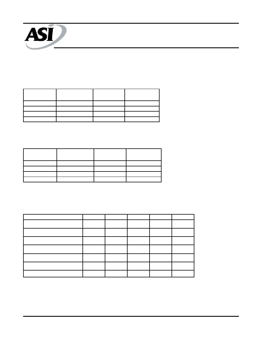
INTERLEAVED BURST ADDRESS TABLE (MODE = NC OR HIGH)
LINEAR BURST ADDRESS TABLE (MODE = LOW)
PARTIAL TRUTH TABLE FOR READ/WRITE COMMANDS*
FUNCTION
R/W\
BWa\
BWb\
BWc\
BWd\
READ
H
X
X
X
X
Write Abort/NOP
L
H
H
H
H
Write Byte a (DQa, DQPa)
2
L
L
H
H
H
Write Byte b (DQb, DQPb)
2
L
H
L
H
H
Write Byte c (DQc, DQPc)
2
L
H
H
L
H
Write Byte d (DQd, DQPd)
2
L
H
H
H
L
Write all bytes
L
L
L
L
L
*
NOTE:
Using R/W\ and byte write(s), any one or more bytes may be written.
SRAM
AS5SS128K36
Austin Semiconductor, Inc.
AS5SS128K36
Rev. 2.0 12/00
Austin Semiconductor, Inc. reserves the right to change products or specifications without notice.
5
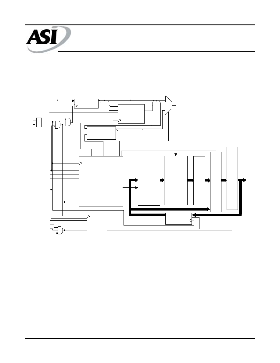
FUNCTIONAL BLOCK DIAGRAM
NOTE:
The Functional Block Diagram illustrates simplified device operation. See Truth Table, pin descriptions and timing diagrams for detailed
information.
17
17
15
17
SA0, SA1, SA
SA1'
SA0'
MODE
ADV/LD\
CLK
K
CKE\
17
ADV/LD\
BWa\
BWb\
DQs
BWc\
BWd\
R/W\
OE\
CE\
CE2
CE2\
O
U
T
P
U
T
B
U
F
F
E
R
S
D
A
T
A
S
T
E
E
R
I
N
G
S
E
N
S
E
A
M
P
S
128K X 9 X 4
MEMORY
ARRAY
WRITE
DRIVERS
WRITE REGISTRY AND
DATA COHERENCY
CONTROL LOGIC
READ
LOGIC
INPUT
REGISTER
WRITE ADDRESS
REGISTER
ADDRESS
REGISTER
BURST
LOGIC
D1
D0
Q1
Q0
SA1
SA0
K
CE
E
E
17
SRAM
AS5SS128K36
Austin Semiconductor, Inc.
AS5SS128K36
Rev. 2.0 12/00
Austin Semiconductor, Inc. reserves the right to change products or specifications without notice.
6
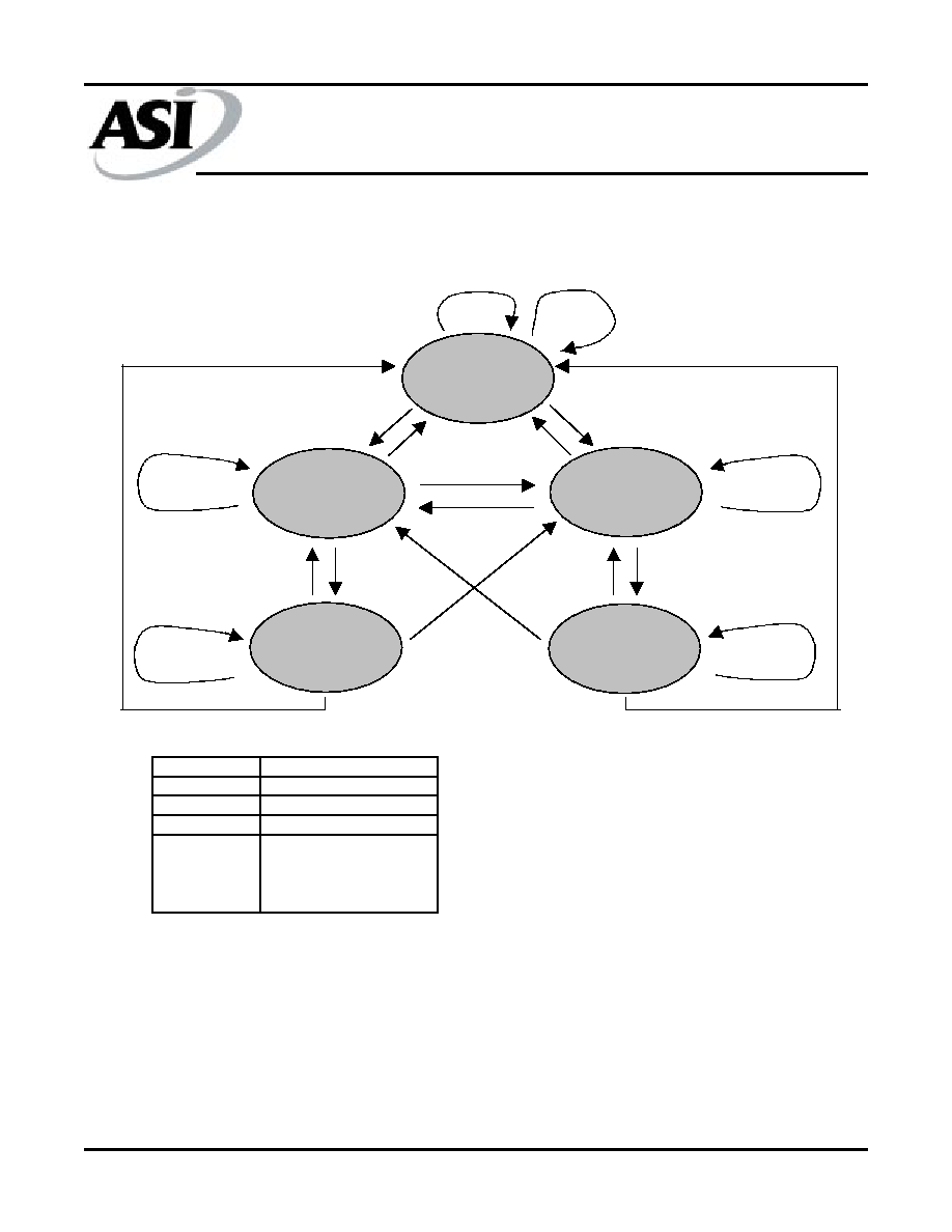
STATE DIAGRAM FOR ZBL SRAM
DS
DS
WRITE
READ
READ
BURST
BURST
WRITE
BEGIN
READ
BURST
READ
BEGIN
WRITE
BURST
WRITE
BURST
READ
BURST
BURST
WRITE
DS
DESELECT
WRITE
READ
WRITE
READ
DS
DS
KEY:
COMMAND
ACTION
DS
DESELECT
READ
New READ
WRITE
New WRITE
BURST
BURST READ,
BURST WRITE or
CONTINUE DESELECT
NOTE:
1. A STALL or IGNORE CLOCK EDGE cycle is not shown in the above diagram. This is because CKE\ HIGH only
blocks the clock (CLK) input and does not change the state of the device.
2. States change on the rising edge of the clock (CLK).
SRAM
AS5SS128K36
Austin Semiconductor, Inc.
AS5SS128K36
Rev. 2.0 12/00
Austin Semiconductor, Inc. reserves the right to change products or specifications without notice.
7
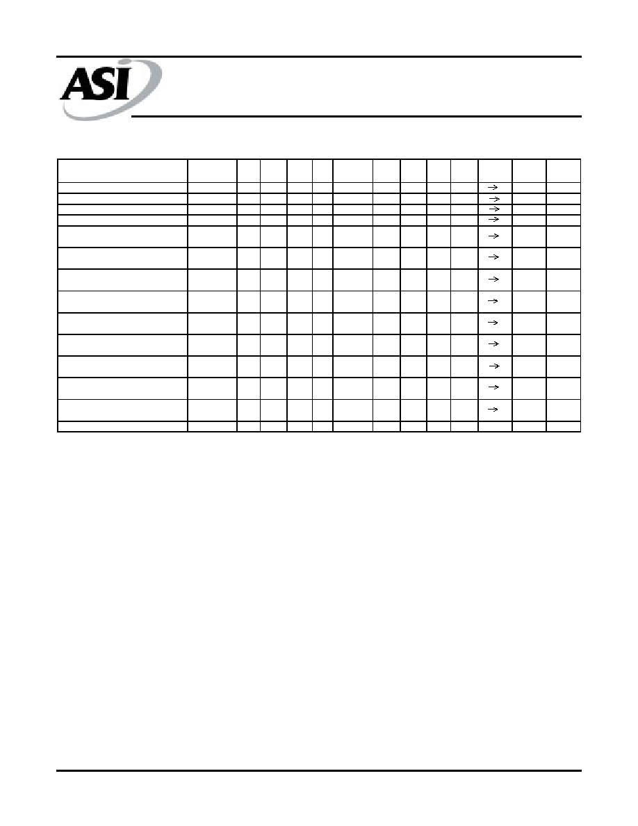
TRUTH TABLE
(5-10
)
NOTE:
1.
CONTINUE BURST cycles, whether READ or WRITE, use the same control inputs. The type of cycle performed (READ
or WRITE) is chosen in the initial BEGIN BURST cycle. A CONTINUE DESELECT cycle can only be entered if a
DESELECT cycle is first executed.
2.
DUMMY READ and WRITE ABORT cycles can be considered NOPs because the device performs no external operation.
A WRITE ABORT means a WRITE command is given, but no operation is performed.
3.
OE\ may be wired LOW to minimize the number of control signals to the SRAM. The device will automatically turn off the
output drivers during a WRITE cycle. OE\ may be used when the bus turn-on and turn-off times do not meet an applications
requirements.
4.
If an IGNORE CLOCK EDGE command occurs during a READ operation, the DQ bus will remain active (Low-Z). If it occurs
during a WRITE cycle, the bus will remain in High-Z. No WRITE operations will be performed during the IGNORE CLOCK
EDGE cycle.
5.
X means "Don't Care." H means logic HIGH. L means logic LOW. BWx = H means all byte write signals (BWa\, BWb\, BWc\,
BWd\) are HIGH. BWx = L means all byte write signals are LOW.
6.
BWa\ enables WRITES to Byte "a" (DQa pins); BWb\ enables WRITES to Byte "b" (DQb pins); BWc\ enables WRITES to
Byte "c" (DQc pins); BWd\ enables WRITES to Byte "d" (DQd pins).
7.
All inputs except OE\ and ZZ must meet setup and hold times around the rising edge (LOW to HIGH) of CLK.
8.
Wait states are inserted by setting CKE\ HIGH.
9.
This device contains circuitry that will ensure that the outputs will be in the High-Z during power-up.
10. The device incorporates a 2-bit burst counter. Address wraps to the initial address every fourth BURST cycle.
11. The address counter is incremented for all CONTINUE BURST cycles.
OPERATION
ADDRESS
USED
CE\
CE2\
CE2
ZZ
ADV/LD\
R/W\
BWx
OE\
CKE\
CLK
DQ
NOTES
DESELECT CYCLE
None
H
X
X
L
L
X
X
X
L
L
H
High-Z
DESELECT CYCLE
None
X
H
X
L
L
X
X
X
L
L
H
High-Z
DESELECT CYCLE
None
X
X
L
L
L
X
X
X
L
L
H
High-Z
CONTINUE DESELECT CYCLE
None
X
X
X
L
H
X
X
X
L
L
H
High-Z
1
READ CYCLE
(Begin Burst)
External
L
L
H
L
L
H
X
L
L
L
H
Q
READ CYCLE
(Continue Burst)
Next
X
X
X
L
H
X
X
L
L
L
H
Q
1, 11
NOP/DUMMY READ
(Begin Burst)
External
L
L
H
L
L
H
X
H
L
L
H
High-Z
2
DUMMY READ
(Continue Burst)
Next
X
X
X
L
H
X
X
H
L
L
H
High-Z
1, 2, 11
WRITE CYCLE
(Begin Burst)
External
L
L
H
L
L
L
L
X
L
L
H
D
3
WRITE CYCLE
(Continue Burst)
Next
X
X
X
L
H
X
L
X
L
L
H
D
1, 3, 11
NOP/WRITE ABORT
(Begin Burst)
None
L
L
H
L
L
L
H
X
L
L
H
High-Z
2, 3
WRITE ABORT
(Continue Burst)
Next
X
X
X
L
H
X
H
X
L
L
H
High-Z
1, 2, 3,
11
IGNORE CLOCK EDGE
(Stall)
Current
X
X
X
L
X
X
X
X
H
L
H
---
4
SNOOZE MODE
None
X
X
X
H
X
X
X
X
X
X
High-Z
SRAM
AS5SS128K36
Austin Semiconductor, Inc.
AS5SS128K36
Rev. 2.0 12/00
Austin Semiconductor, Inc. reserves the right to change products or specifications without notice.
8
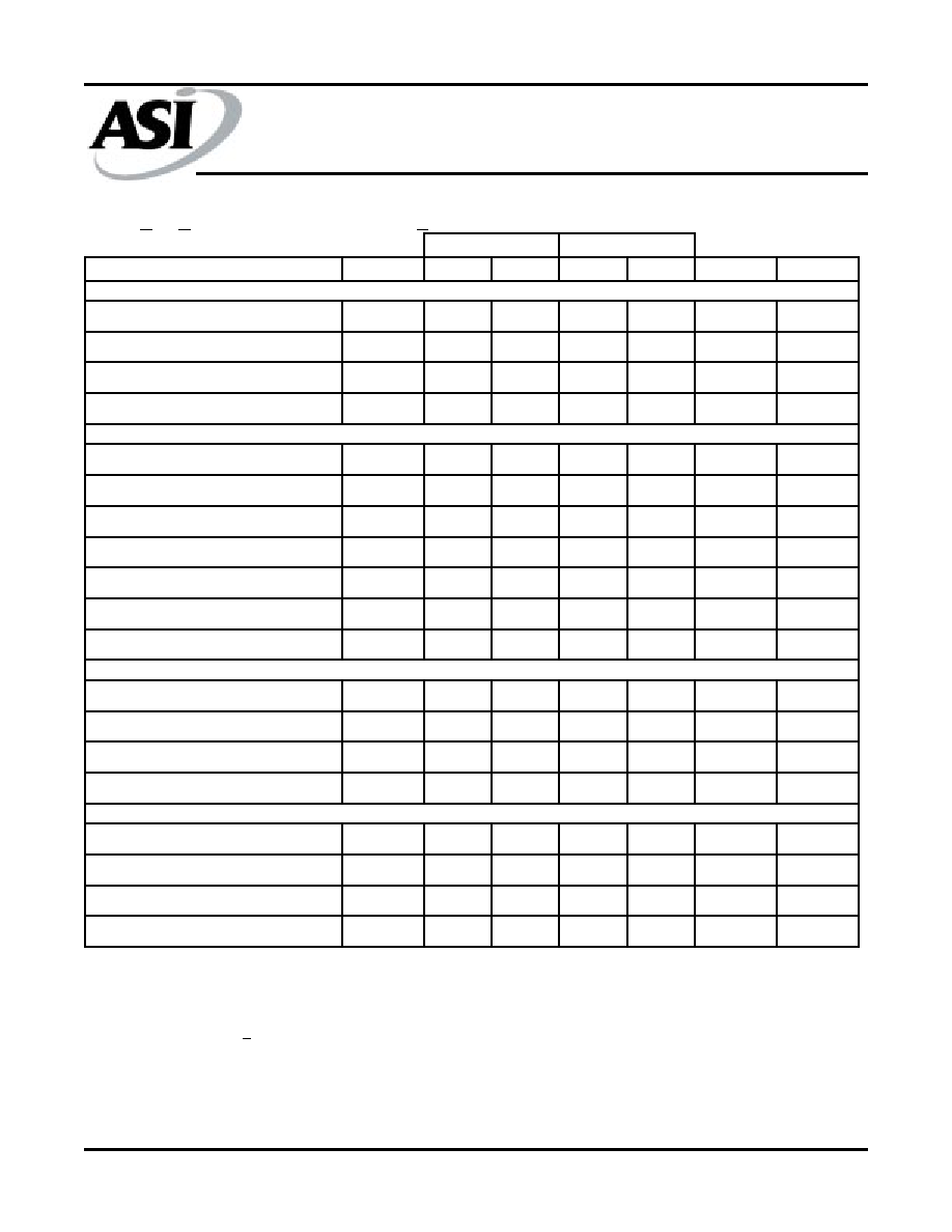
ABSOLUTE MAXIMUM RATINGS*
Voltage on V
DD
Supply Relative to V
SS
.................-0.5V to +4.6V
Voltage on V
DD
Q Supply Relative to V
SS
.................-0.5V to V
DD
V
IN
.................................................................. -0.5V to V
DD
Q +0.5V
Storage Temperature (Plastics) ..........................-55
∞
C to +150
∞
C
Short Circuit Output Current .............................................100mA
Max. Junction Temperature*.............................................+150
∞
C
*Stresses greater than those listed under "Absolute Maximum Rat-
ings" may cause permanent damage to the device. This is a stress
rating only and functional operation of the device at these or any other
conditions above those indicated in the operation section of this speci-
fication is not implied. Exposure to absolute maximum rating condi-
tions for extended periods may affect reliability.
**Junction Temperature depends upon package type, cycle time, load-
ing, ambient temperture and airflow.
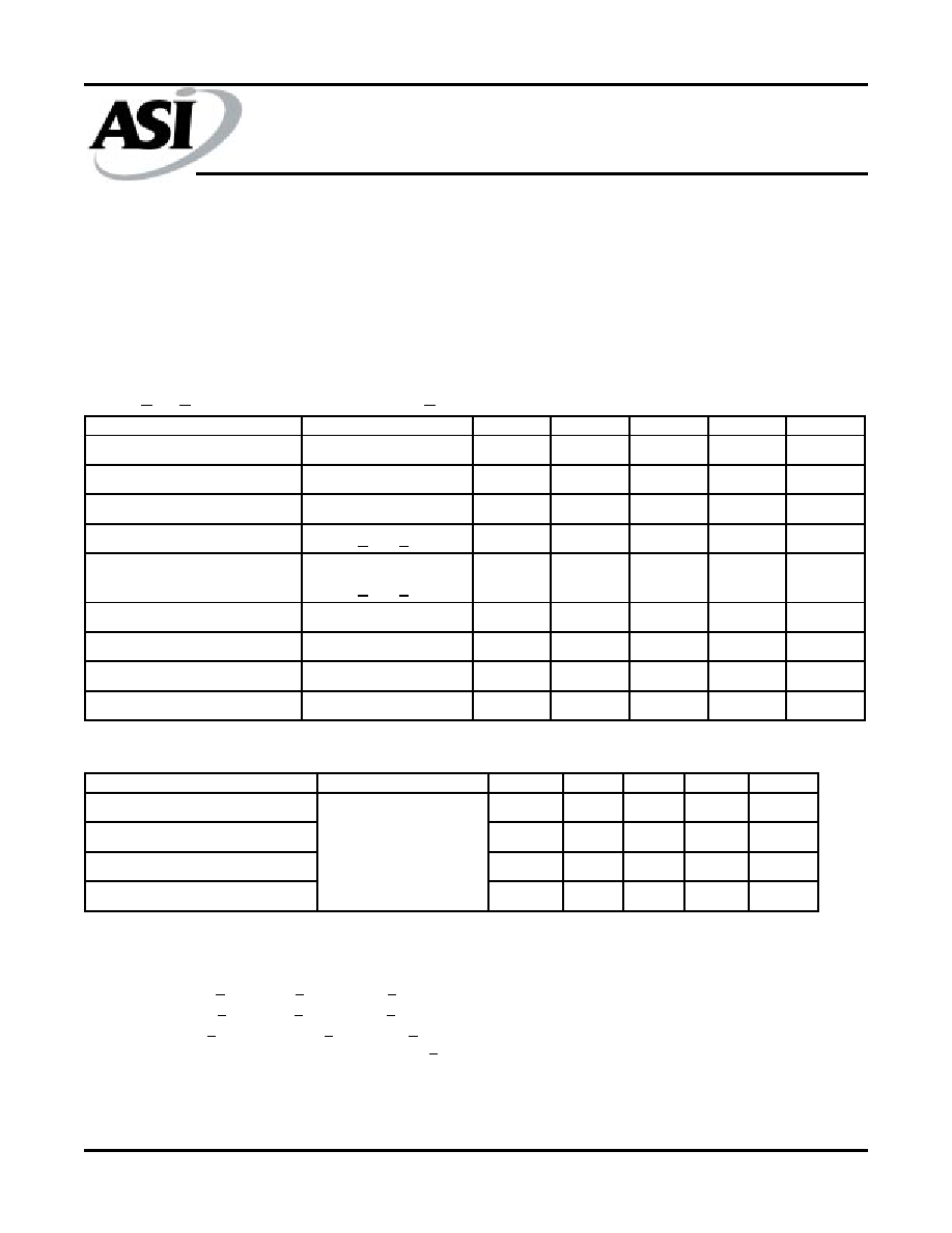
DC ELECTRICAL CHARACTERISTICS AND RECOMMENDED OPERATING CONDITIONS
(-55
o
C < T
A
< +125
o
C; V
DD,
V
DD
Q = +3.3V +0.165V unless otherwise noted)
NOTE:
1.
All voltages referenced to V
SS
(GND).
2.
Overshoot: V
IH
< +4.6V for t < t
KHKH
/2 for I < 20mA.
Undershoot: V
IL
< -0.7V for t < t
KHKH
/2 for I < 20mA.
Power-up: V
IH
< +3.465V and V
DD
< 3.135V for t < 200ms.
3.
MODE pin has an internal pull-up, and input leakage = + 10
µ
A.
4.
The load used for V
OH
, V
OL
testing is shown in Figure 2. AC load current is higher than the shown DC values. AC I/O curvers
are available upon request.
5.
V
DD
Q should never exceed V
DD
. V
DD
and V
DD
Q should be externally wired together to the same power supply.
6.
This parameter is sampled.
DESCRIPTION
CONDITIONS
SYMBOL
MIN
MAX
UNITS
NOTES
Input High (Logic 1) Voltage
V
IH
2.0
V
DD
+ 0.3
V
1, 2
Input High (Logic 1) Voltage
DQ Pins
V
IH
2.0
V
DD
+ 0.3
V
1, 2
Input Low (Logic 0) Voltage
V
IL
-0.3
0.8
V
1, 2
Input Leakage Current
0V < V
IN
< V
DD
IL
I
-1.0
1.0
µ
A
3
Output Leakage Current
Output(s) Disabled,
0V < V
IN
< V
DD
IL
O
-1.0
1.0
µ
A
Output High Voltage
I
OH
= -4.0mA
V
OH
2.4
---
V
1, 4
Output Low Voltage
I
OL
= 8.0mA
V
OL
---
0.4
V
1, 4
Supply Voltage
V
DD
3.135
3.465
V
1
Isolated Output Buffer Supply
V
DD
Q
3.135
V
DD
V
1, 5
CAPACITANCE
DESCRIPTION
CONDITIONS
SYMBOL
TYP
MAX
UNITS
NOTES
Control Input Capacitance
C
I
3
4
pF
6
Input/Output Capacitance (DQ)
C
O
4
5
pF
6
Address Capacitance
C
A
3
3.5
pF
6
Clock Capacitance
C
CK
3
3.5
pF
6
T
A
= 25
o
C; f = 1 MHz
V
DD
= 3.3V
SRAM
AS5SS128K36
Austin Semiconductor, Inc.
AS5SS128K36
Rev. 2.0 12/00
Austin Semiconductor, Inc. reserves the right to change products or specifications without notice.
9
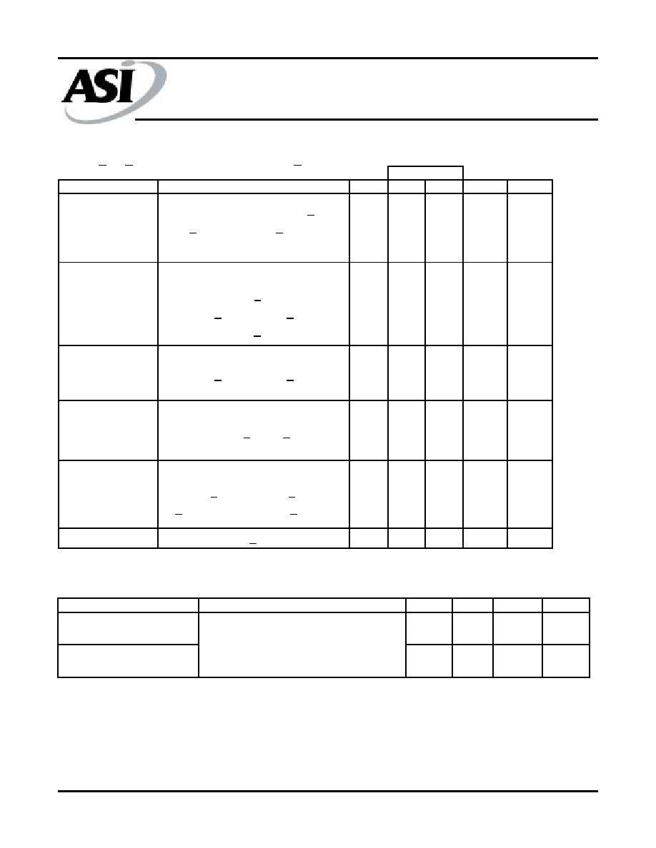
DESCRIPTION
CONDITIONS
SYM
-11
-12
UNITS NOTES
Power Supply
Current: Operating
Device selected; All inputs < V
IL
or > V
IH
; Cycle time > t
KC
(MIN)
V
DD
= MAX; Outputs open
I
DD
275
250
mA
1, 2
Power Supply
Current: Idle
Device selected; V
DD
= MAX;
CKE\ > V
IH
;
All inputs < V
SS
+ 0.2 or > V
DD
-0.2;
Cycle time > t
KC
(MIN)
I
DD1
22
20
mA
1, 2
CMOS Standby
Device selected; V
DD
= MAX;
All inputs < V
SS
+ 0.2 or > V
DD
-0.2;
All inputs static; CLK frequency = 0
I
SB2
10
10
mA
2
TTL Standby
Device selected; V
DD
= MAX;
All inputs < V
IL
or > V
IH
;
All inputs static; CLK frequency = 0
I
SB3
25
25
mA
2
Clock Running
Device selected; V
DD
= MAX;
ADV/LD\ > V
IH
; All inputs < V
SS
+ 0.2
or > V
DD
- 0.2; Cycle time > t
KC
(MIN)
I
SB4
65
60
mA
2
Snooze Mode
ZZ > V
IH
I
SB2Z
10
10
mA
2
MAX
I
DD
OPERATING CONDITIONS AND MAXIMUM LIMITS
(-55
o
C < T
A
< +125
o
C; V
DD,
V
DD
Q = +3.3V +0.165V unless otherwise noted)
THERMAL RESISTANCE
DESCRIPTION
CONDITIONS
SYM
TYP
UNITS
NOTES
Thermal Resistance
(Junction to Ambient)
JA
46
o
C/W
3
Thermal Resistance
(Junction to Top of Case)
JC
2.8
o
C/W
3
Test conditions follow standard test
methods and procedures for measuring
thermal impedance, per EIA/JESD51
NOTE:
1.
I
DD
is specified with no output current and increases with faster cycle times. I
DD
Q increases with faster cycle times and
greater output loading.
2.
"Device deselected" means device is in a deselected cycle as defined in the truth table. "Device selected" means device
is active (not in deselected mode).
3.
This parameter is sampled.
SRAM
AS5SS128K36
Austin Semiconductor, Inc.
AS5SS128K36
Rev. 2.0 12/00
Austin Semiconductor, Inc. reserves the right to change products or specifications without notice.
10
DESCRIPTION
SYM
MIN
MAX
MIN
MAX
UNITS
NOTES
CLOCK
Clock cycle time
t
KHKH
11
12
ns
Clock frequency
t
KF
90
83
MHz
Clock HIGH time
t
KHKL
3.0
3.0
ns
1
Clock LOW time
t
KLKH
3.0
3.0
ns
1
OUTPUT TIMES
Clock to output valid
t
KHQV
8.5
9.0
ns
Clock to output invalid
t
KHQX
3.0
3.0
ns
2
Clock to output in Low-Z
t
KHQX1
3.0
3.0
ns
2, 3, 4, 5
Clock to output in High-Z
t
KHQZ
5.0
5.0
ns
2, 3, 4, 5
OE\ to output valid
t
GLQV
5.0
5.0
ns
6
OE\ to output in Low-Z
t
GLQX
0
0
ns
2, 3, 4, 5
OE\ to output in High-Z
t
GHQZ
5.0
5.0
ns
2, 3, 4, 5
SETUP TIMES
Address
t
AVKH
2.2
2.5
ns
7
Clock enable (CKE\)
t
EVKH
2.2
2.5
ns
7
Control signals
t
CVKH
2.2
2.5
ns
7
Data-in
t
DVKH
2.2
2.5
ns
7
HOLD TIMES
Address
t
KHAX
0.5
0.5
ns
7
Clock enable (CKE\)
t
KHEX
0.5
0.5
ns
7
Control signals
t
KHCX
0.5
0.5
ns
7
Data-in
t
KHDX
0.5
0.5
ns
7
-11
-12
AC ELECTRICAL CHARACTERISTICS
6, 8, 9
(-55
o
C < T
A
< +125
o
C; V
DD,
V
DD
Q = +3.3V +0.165V)
NOTE:
1 .
Measured as HIGH above V
IH
and LOW below V
IL
.
2 .
Contact ASI for more information on these parameters.
3.
This parameter is sampled.
4 .
This parameter is measured with the output loading shown in Figure 2.
5 .
Transistion is measured +200mV from steady state voltage.
6 .
OE\ can be considerted a "Don't Care" during WRITEs; however, controlling OE\ can help fine-tune a system for ZBL timing.
7 .
This is a synchrnous device. All addresses must meet the specified setup and hold times for all rising edgges o CLK when they are being
registered into the device. All other synchronous inputs must meet the setup and hold times with stable logic levels for all rising edges of
clock (CLK) when the chip is enabled. Chip enable must be valid at each rising edge of CLK when ADV/LD\ is LOW to remain enabled.
8 .
Test conditions as specified with the output loading shown in Figure 1, unless otherwise noted.
9 .
A WRITE cycle is defined by R/W\ LOW having been registered into the device at ADV/LD\ LOW. A READ cycle is defined by R/W\
HIGH with ADV/LD\ LOW. Both cases must meet setup and hold times.
SRAM
AS5SS128K36
Austin Semiconductor, Inc.
AS5SS128K36
Rev. 2.0 12/00
Austin Semiconductor, Inc. reserves the right to change products or specifications without notice.
11
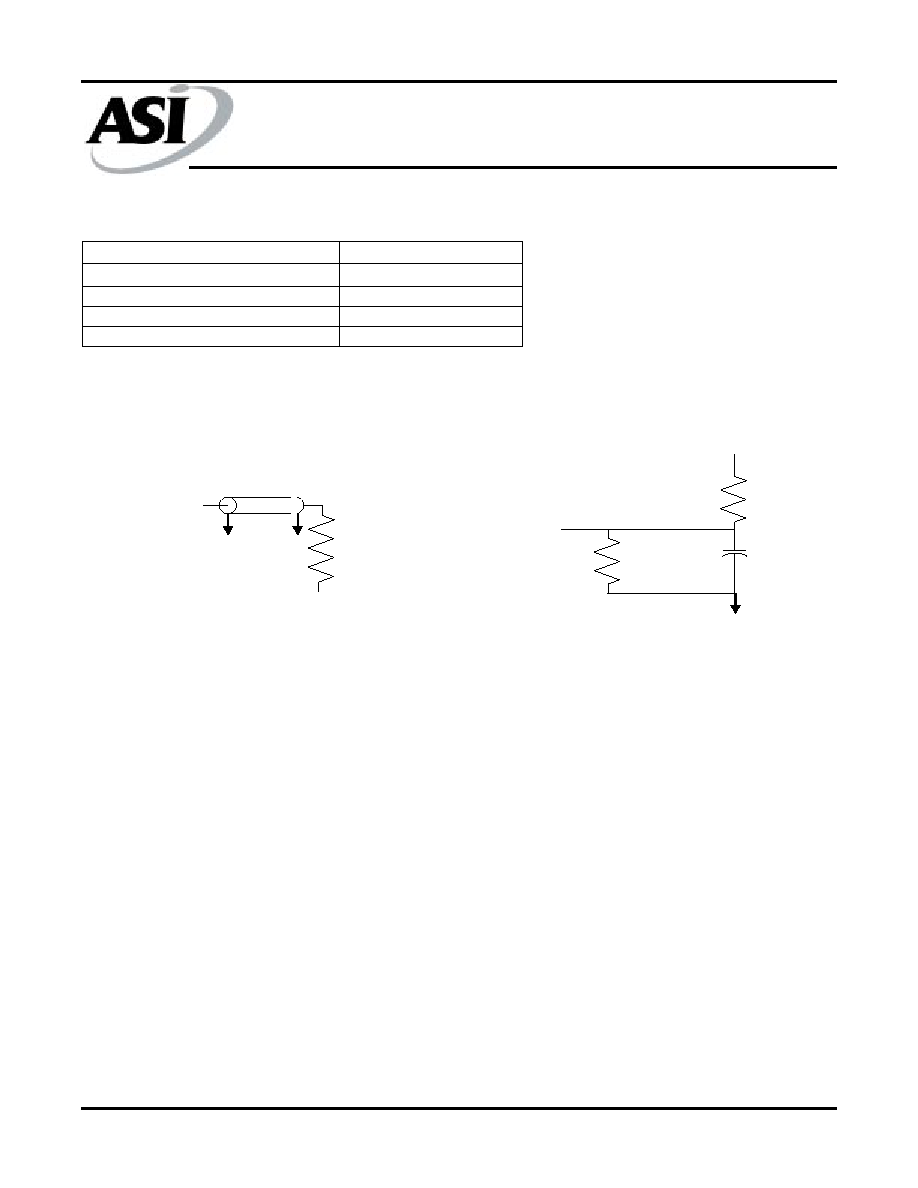
AC TEST CONDITIONS
OUTPUT LOADS
Fig. 2 OUTPUT LOAD EQUIVALENT
Fig. 1 OUTPUT LOAD EQUIVALENT
Input pulse levels
Input timing reference levels
Input slew rate
Output reference levels
Output load
Vss to 3.3V
1.5V
1 ns
1.5V
See Figures 1 and 2
3.3v
Q
351
5 pF
317
Q
50
Z
0
=50
V
T
= 1.5V
LOAD DERATING CURVES
The ASI 128K x 36 ZBL SRAM timing is dependent upon
the capacitive loading on the outputs.
Consult the factory for copies of I/O current versus
voltage curves.
SRAM
AS5SS128K36
Austin Semiconductor, Inc.
AS5SS128K36
Rev. 2.0 12/00
Austin Semiconductor, Inc. reserves the right to change products or specifications without notice.
12
SNOOZE MODE
SNOOZE MODE is a low-current, "power-down" mode
in which the device is deselected and current is reduced to
I
SB2Z
. The duration of SNOOZE MODE is dictated by the
length of time the ZZ pin is in a HIGH state. After the device
enters SNOOZE MODE, all inputs except ZZ become dis-
abled and all outputs go to High-Z.
The ZZ pin is an asynchronous, active HIGH input that
causes the device to enter SNOOZE MODE. When the ZZ pin
becomes a logic HIGH, I
SB2Z
is guaranteed after the time t
ZZI
is met. Any READ or WRITE operation pending when the
device enters SNOOZE MODE is not guaranteed to complete
sucessfully. Therefore, SNOOZE MODE must not be initiated
until valid pending operations are completed. Similarly, when
exiting SNOOZE MODE during t
RZZ
, only a DESELECT or READ
cycle should be given.
SNOOZE MODE ELECTRICAL CHARACTERISTICS
DESCRIPTION
CONDITIONS
SYM
MIN
MAX
UNITS NOTES
Current during SNOOZE MODE
ZZ > V
IH
I
SB2Z
10
mA
ZZ active to input ignored
t
ZZ
0
t
KHKH
ns
1
ZZ inactive to input sampled
t
RZZ
0
t
KHKH
ns
1
ZZ active to snooze current
t
ZZI
t
KHKH
ns
1
ZZ inactive to exit snooze current
t
RZZI
0
ns
1
SNOOZE MODE WAVEFORM
CLK
ZZ
I
SUPPLY
ALL INPUTS
(except ZZ)
Outputs (Q)
12345
12345
12345
12345
12345
12345678901234567890
12345678901234567890
12345678901234567890
12345678901234567890
12345678901234567890
12
12
12
12
12
12345
12345
12345
12345
12345678901234567890
12345678901234567890
12345678901234567890
12345678901234567890
12
12
12
12
123456
123456
123456
123456
123456
12345
12345
12345
12345
12345
123456789012345678901
123456789012345678901
123456789012345678901
123456789012345678901
123456789012345678901
12
12
12
12
12
12
12
12
12
12
DESELECT
or READ Only
1
12
t
RZZ
1
1
t
ZZ
1
1
t
ZZI
I
ISB2Z
High-Z
1
12
t
RZZI
12345
12345
12345
12345
12345
Don't Care
SRAM
AS5SS128K36
Austin Semiconductor, Inc.
AS5SS128K36
Rev. 2.0 12/00
Austin Semiconductor, Inc. reserves the right to change products or specifications without notice.
13
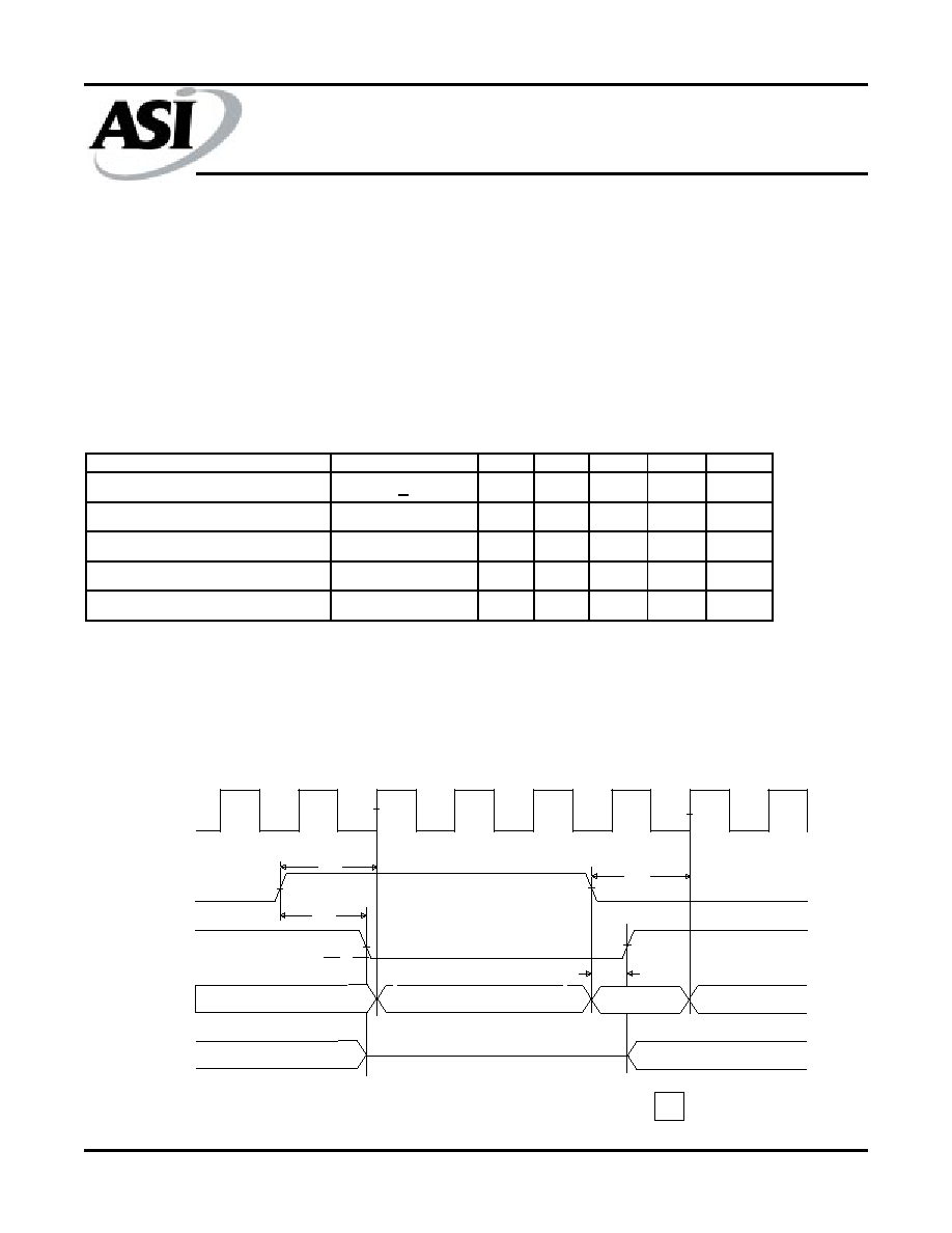
READ/WRITE TIMING
READ/WRITE TIMING PARAMETERS
MIN
MAX
MIN
MAX
t
KHKH
11
12
t
KF
90
83
t
KHKL
3.0
3.0
t
KLKH
3.0
3.0
t
KHQV
8.5
9.0
t
KHQX
3.0
3.0
t
KHQX1
3.0
3.0
t
KHQZ
5.0
5.0
t
GLQV
5.0
5.0
t
GLQX
0
0
SYMBOL
-12
-11
MIN
MAX
MIN
MAX
t
GHQZ
5.0
5.0
t
AVKH
2.2
2.5
t
EVKH
2.2
2.5
t
CVKH
2.2
2.5
t
DVKH
2.2
2.5
t
KHAX
0.5
0.5
t
KHEX
0.5
0.5
t
KHCX
0.5
0.5
t
GLDX
0.5
0.5
SYMBOL
-12
-11
NOTE:
1. For this waveform, ZZ is tied LOW.
2. Burst sequence order is determined by MODE (0=linear, 1=interleaved). BURST operations are optional.
3. CE\ represents three signals. When CE\ = 0, it represents CE\ = 0, CE2\ = 0, CE2 = 1.
4. Data coherency is provided for all possible operations. If a READ is initiated, the most current data is used. The most
recent data may be from the input data register.
1234
1234
1234
1234
1234
1234
1234
1234
1234
1234
1234
1234
1234
123
123
123
1234
1234
1234
1234
1234
1234
123
123
123
123
123
123
1234
1234
1234
1234
1234
1234
1234
1234
1234
1234
1234
1234
1234
1234
12
12
12
1
1
1
123456789
123456789
123456789
12
12
12
1
1
1
12
12
12
12
12
12
12345678
12345678
12345678
12
12
12
12
12
12
1234
1234
1234
1234
1234
1234
1234
1234
1234
1234
1234
1234
1234
1234
1234
1234
1234
1234
1234
1234
1234
1234
1234
1234
1234
1234
1234
1234
1234
1234
1234
1234
1234
1234
1234
123
123
123
123
1234
1234
1234
1234
1234
1234
1234
1234
1234
1234
1234
1234
1234
1234
1234567890
1234567890
1234567890
1234
1234
1234
1234
1234567890
1234567890
1234567890
1234
1234
1234
1234
1234
1234
1234567890
1234567890
1234567890
1234
1234
1234
1234
1234
1234
1234
1234
1234
1
1
12
12
123456789012345678901
123456789012345678901
123456789012345678901
12
12
12
12
12
12
12
12
12
12
12345678
12345678
12345678
12
12
12
12
12
12
123456789
123456789
123456789
1234
1234
1234
A1
1234
1234
1234
A2
123
123
123
123
123
123
1234567
1234567
1234567
1
1
1
12
12
12
A3
123
123
123
A4
123
123
123
123
123
123
1234567
1234567
1234567
12
12
12
1
1
1
A5
123
123
123
A6
123
123
123
A7
123
123
123
1234567
1234567
1234567
1
1
1
1234
1234
1234
D(A1)
123
123
123
D(A2)
123
123
123
D(A2+1)
123
123
123
123
Q(A3)
12
12
12
12
Q(A4)
12
12
12
12
Q(A4+1)
123
123
123
123
D(A5)
12
12
12
12
Q(A6)
123
123
123
123
123
123
123
123
D(A7)
WRITE
D(A1)
WRITE
D(A2)
BURST
WRITE
D(A2+1)
READ
Q(A3)
READ
Q(A4)
BURST
READ
Q(A4 +1)
WRITE
D(A5)
READ
Q(A6)
WRITE
D(A7)
DESELECT
123
123
123
Don't Care
1234
1234
1234
1234
Undefined
CLK
CLE\
CE\
ADV/LD\
R/W\
BWx\
ADDRESS
DQ
OE\
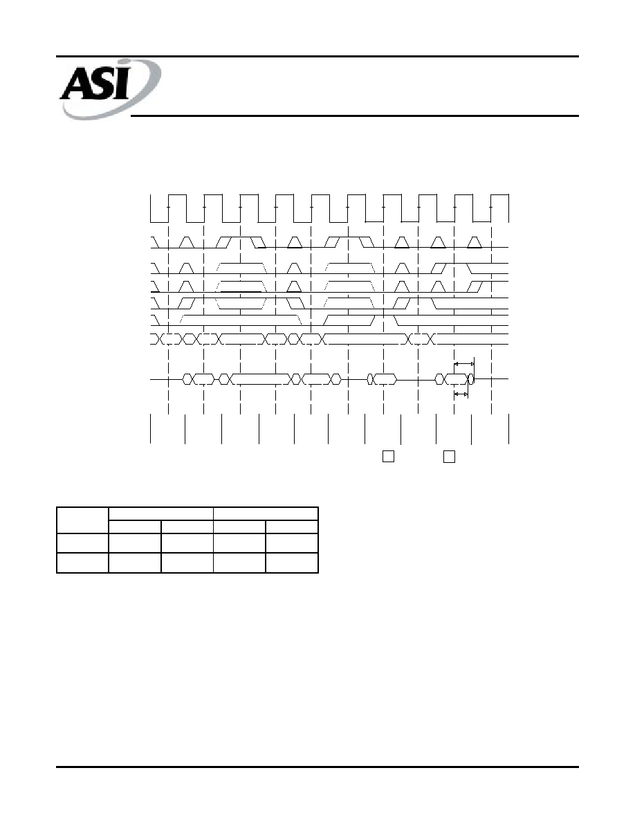
COMMAND
1
2 3 4 5 6 7 8 9 10
t
KHKH
t
KHKL
t
KLKH
t
EVKH
t
KHEX
t
CVKH
t
KHCX
t
AVKH
t
KHAX
t
DVKH
t
KHDX
t
KHQX1
t
KHQV
t
KHQX
t
GHQZ
t
GLQX
t
GLQV
t
KHQX
t
KHQZ
SRAM
AS5SS128K36
Austin Semiconductor, Inc.
AS5SS128K36
Rev. 2.0 12/00
Austin Semiconductor, Inc. reserves the right to change products or specifications without notice.
14
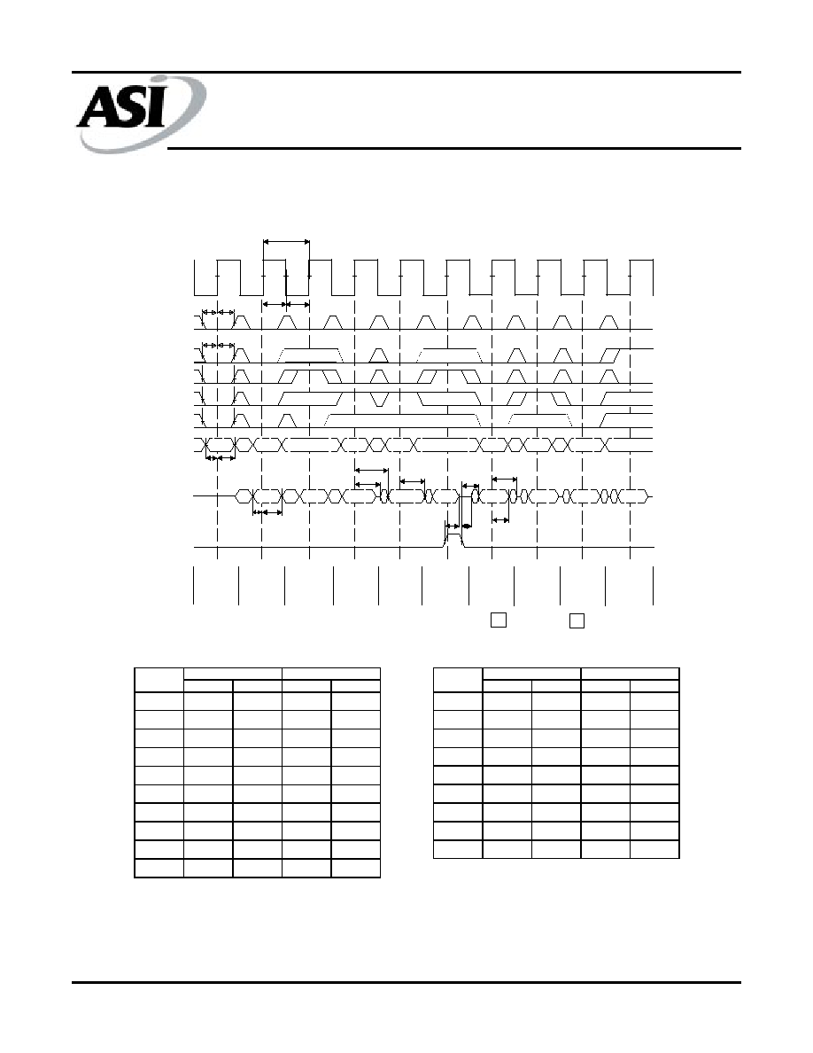
NOP, STALL AND DESELECT CYCLES
123
123
123
123
1234
1234
1234
1234
1234
1234
1234
1234
1234
1234
1234
1234
1234
1234567890123456
1234567890123456
1234567890123456
1234
1234
1234
1234
12
12
12
12
12
12
1234567890123456789012
1234567890123456789012
1234567890123456789012
12
12
12
12
12
12
12345678901234567890123
12345678901234567890123
12345678901234567890123
A1
A2
A3
123
123
123
A4
123
123
123
123
123
123
12345678901234
12345678901234
12345678901234
1
1
1
12
12
12
A5
123
123
123
12345678901234
12345678901234
12345678901234
1
1
1
123
123
123
D(A1)
1234
1234
1234
1234
Q(A2)
123
123
123
123
Q(A3)
123
123
123
123
Q(A5)
12
12
12
12
WRITE
D(A1)
READ
Q(A2)
STALL
READ
Q(A3)
WRITE
D(A4)
STALL
NOP
READ
Q(A5)
DESELECT CONTINUE
DESELECT
123
123
123
Don't Care
1234
1234
1234
1234
Undefined
CLK
CE\
ADV/LD\
R/W\
BWx\
ADDRESS
DQ
COMMAND
1
2 3 4 5 6 7 8 9 10
t
KHQX
t
KHQZ
1234
1234
1234
1234
1234
1234
1234
1234
1234
1234
1234
1234
123
123
123
123
1234
1234
1234
1234
123
123
123
123
1234
1234
1234
1234
1234
1234
1234
1234
1234
1234
1234
1234
CKE\
1234
1234
1234
1234
1234
1234
1234
1234
1234
1
1
12
12
12345678
12345678
12345678
12
12
12
12
12
123
123
123
1234
1234
1234
1234
1234
1234
1234
1234
1234
1234
1234
1234
1234
1234
1234
12
12
12
12
12
12
12345678
12345678
12345678
12
12
12
12
12
12
1
1
1
12
12
12
123456789
123456789
123456789
12
12
12
12
12
12
123
123
123
123
1234
1234
1234
1234
1234
1234
1234
123456789
123456789
12
12
12
12
12345678
12345678
12345678
12
12
12
12
12
12
12
12
12
12
12
12
12345678
12345678
12345678
12
12
12
12
12
12
1
1
1
12
12
12
123456789
123456789
123456789
1
1
1
12
12
12
1234567890
1234567890
1234567890
12
12
12
12
D(A4)
NOP, STALL AND DESELECT TIMING PARAMETERS
MIN
MAX
MIN
MAX
t
KHQX
3.0
3.0
t
KHQZ
5.0
5.0
SYMBOL
-12
-11
NOTE:
1.
The IGNORE CLOCK EDGE or STALL cycle (clock 3) illustrates CKE\ being used to create a "pause". A WRITE is not performed
during this cycle.
2.
For this waveform, ZZ and OE\ are tied LOW.
3.
CE\ represents three signals. When CE\ = 0, it represents CE\ = 0, CE2\ = 0, CE2 = 1.
4.
Data coherency is provided for all possible operations. If a READ is initiated, the most current data is used. The most recent data
may be from the input data register.
SRAM
AS5SS128K36
Austin Semiconductor, Inc.
AS5SS128K36
Rev. 2.0 12/00
Austin Semiconductor, Inc. reserves the right to change products or specifications without notice.
15
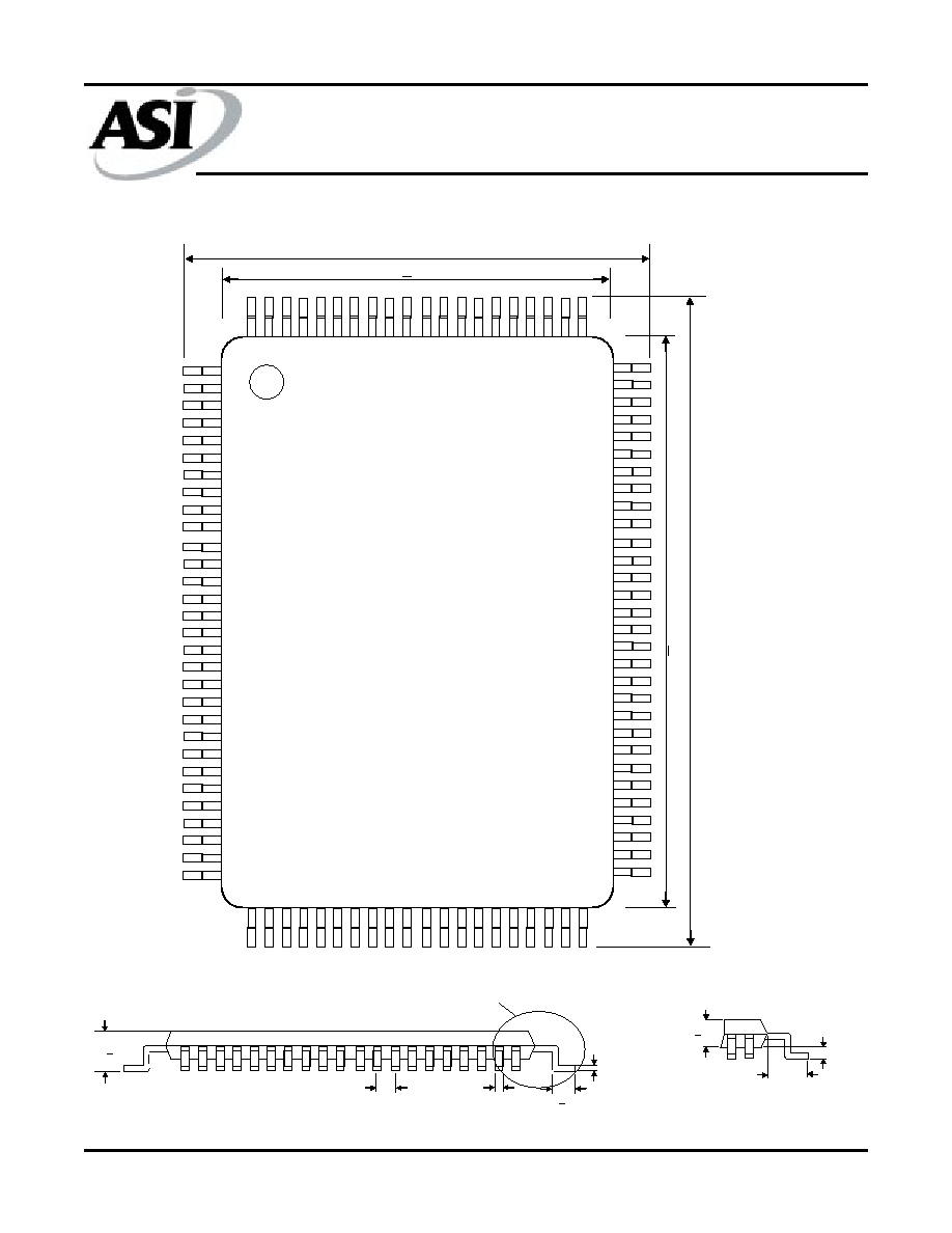
ASI Case # 1001 (Package Designator DQ)
NOTE:
All dimensions in Millimeters.
Detail A
1.40 + 0.05
0.10+0.10/-0.05
1.00 TYP
0.60 + 0.15
0.32+0.06/-0.10
0.65 Basic
1.50 + 0.10
See Detail A
0.15 +0.03/-0.02
16.00 +0.20/-0.05
14.00 + 0.10
22.10 +0.10/-0.15
20.10
+ 0.10
SRAM
AS5SS128K36
Austin Semiconductor, Inc.
AS5SS128K36
Rev. 2.0 12/00
Austin Semiconductor, Inc. reserves the right to change products or specifications without notice.
16
ORDERING INFORMATION
*AVAILABLE PROCESSES
IT = Industrial Temperature Range
-40
o
C to +85
o
C
XT = Extended Temperature Range
-55
o
C to +125
o
C
EXAMPLE: AS5SS128K36DQ-11/IT
Device Number
Package
Type
Speed ns
Process
AS5SS128K36
DQ
-11
/*
AS5SS128K36
DQ
-12
/*