EEPROM
AS8E128K32
Austin Semiconductor, Inc.
AS8E128K32
Rev. 5.5 9/01
Austin Semiconductor, Inc. reserves the right to change products or specifications without notice.
1
GENERAL DESCRIPTION
The Austin Semiconductor, Inc. AS8E128K32 is a 4 Megabit
EEPROM Module organized as 128K x 32 bit. User configurable to
256K x16 or 512Kx 8. The module achieves high speed access, low
power consumption and high reliability by employing advanced CMOS
memory technology.
The military grade product is manufactured in compliance to the
SMD and MIL-STD 883, making the AS8E128K32 ideally suited for
military or space applications.
The module is offered in a 1.075 inch square ceramic pin grid
array substrate. This package design provides the optimum space
saving solution for boards that accept through hole packaging.
The module is also offered as a 68 lead 0.990 inch square ceramic
quad flat pack. It has a max. height of 0.200 inch. This package design
is targeted for those applications which require low profile SMT
Packaging.
FEATURES
�
Access times of 120, 140, 150, 200, 250, and 300 ns
�
Built in decoupling caps for low noise operation
�
Organized as 128K x32; User configurable
as 256K x16 or 512K x8
�
Operation with single 5 volt supply
�
Low power CMOS
�
TTL Compatible Inputs and Outputs
�
Operating Temperature Ranges:
Military: -55
o
C to +125
o
C
Industrial: -40
o
C to +85
o
C
OPTIONS
MARKINGS
�
Timing
120 ns
-120
140 ns
-140
150 ns
-150
200 ns
-200
250 ns
-250
300 ns
-300
�
Package
Ceramic Quad Flat pack
Q
No. 703
Pin Grid Array- 8 Series
P
No. 904
Pin Grid Array- 8 Series
PN
No. 904
AVAILABLE AS MILITARY
SPECIFICATIONS
�
SMD 5962-94585
�
MIL-STD-883
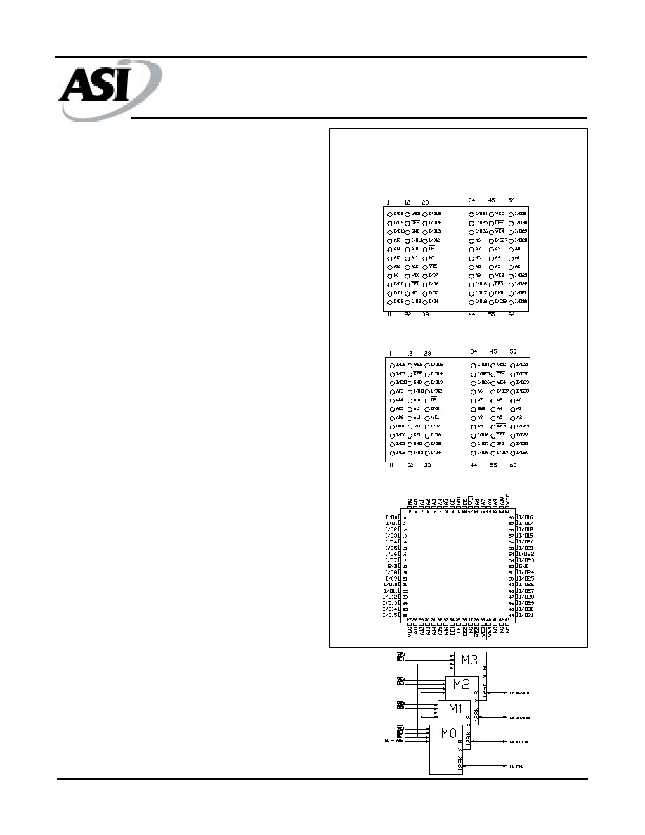
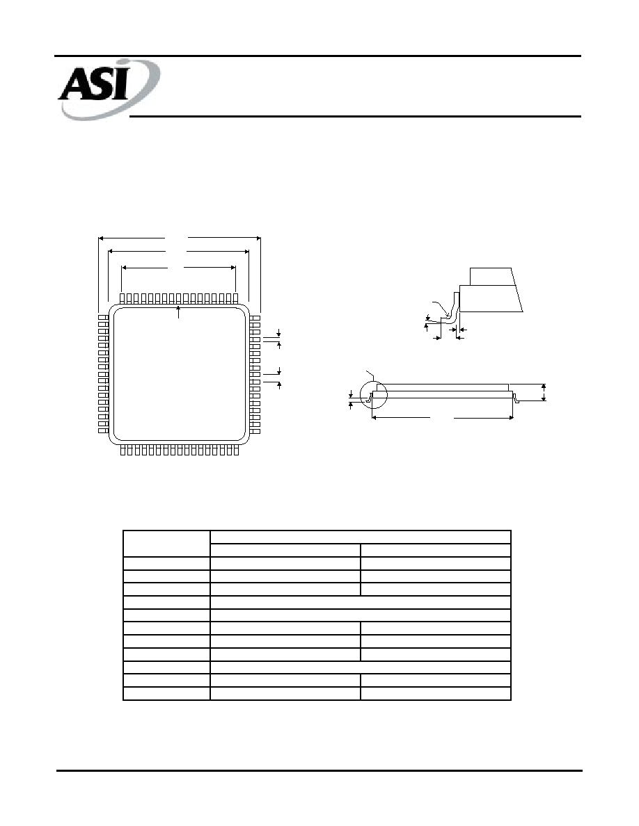
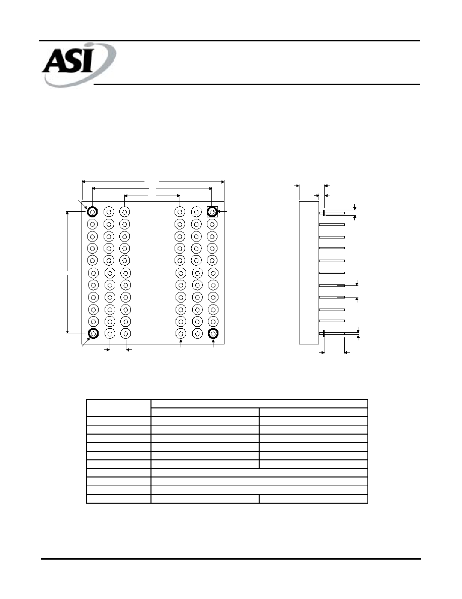
PIN ASSIGNMENT
(Top View)
66 Lead PGA
(Pins 8, 21, 28, 39 are no connects on the PN package)
68 Lead CQFP
66 Lead PGA
(Pins 8, 21, 28, 39 are grounds on the P package)
128K x 32 EEPROM
EEPROM Memory Array
For more products and information
please visit our web site at
www.austinsemiconductor.com
3
4

EEPROM
AS8E128K32
Austin Semiconductor, Inc.
AS8E128K32
Rev. 5.5 9/01
Austin Semiconductor, Inc. reserves the right to change products or specifications without notice.
2
of the last byte written will result in the complement of the written
data to be presented on I/O7. Once the write cycle has been com-
pleted, true data is valid on all outputs, and the next write cycle may
begin. DATA Polling may begin at anytime during the write cycle.
TOGGLE BIT
In addition to DATA Polling the module provides another method
for determining the end of a write cycle. During the write operation,
successive attempts to read data from the device will result in I/O6 of
the accessed die toggling between one and zero. Once the write has
completed, I/O6 will stop toggling and valid data will be read. Reading
the toggle bit may begin at any time during the write cycle.
DATA PROTECTION
If precautions are not taken, inadvertent writes may occur during
transitions of the host power supply. The E
2
module has incorpo-
rated both hardware and software features that will protect the memory
against inadvertent writes.
HARDWARE PROTECTION
Hardware features protect against inadvertent writes to the mod-
ule in the following ways: (a) Vcc sense - if Vcc is below 3.8 V
(typical) the write function is inhibited; (b) Vcc power-on delay -
once Vcc has reached 3.8 V the device will automatically time out 5 ms
(typical) before allowing a write; (c) write inhibit - holding any one of
OE\ low, CE\ high or WE\ high inhibits write cycles; (d) noise filter -
pulses of less than 15 ns (typical) on the WE\ or CE\ inputs will not
initiate a write cycle.
SOFTWARE DATA PROTECTION
A software controlled data protection feature has been imple-
mented on the memory module. When enabled, the software data
protection (SDP), will prevent inadvertent writes. The SDP feature
may be enabled or disabled by the user and is shipped with SDP
disabled, SDP is enabled by the host system issuing a series of three
write commands; three specific bytes of data are written to three
specific addresses (refer to Software Data Protection Algorithm). After
writing the three byte command sequence and after t
WC
the entire
module will be protected from inadvertent write operations. It should
be noted, that once protected the host may still perform a byte of page
write to the module. This is done by preceding the data to be written
by the same three byte command sequence used to enable SDP. Once
set, SDP will remain active unless the disable command sequence is
issued. Power transitions do not disable SDP and SDP will protect
the 128K x 32 EEPROM during power-up and Power-down condi-
tions. All command sequences must conform to the page write timing
specifications. The data in the enable and disable command sequences
is not written to the device and the memory addresses used in the
sequence may be written with data in either a byte or page write
operation.
After setting SDP, any attempt to write to the device without the
three byte command sequence will start the internal write timers. No
data will be written to the device; however, for the duration of t
WC
,
read operations will effectively be polling operations.
DEVICE IDENTIFICATION
An extra 128 bytes of EEPROM memory is available on each
die for user identification. By raising A9 to 12V + 0.5V and using
address locations 1FF80H to 1FFFFH the bytes may be written to
or read from in the same manner as the regular memory array.
DEVICE OPERATION
The 128K x 32 EEPROM memory solution is an electrically
erasable and programmable memory module that is accessed like a
Static RAM for the read or write cycle without the need for external
components. The device contains a 128-byte-page register to allow
writing of up to 128 bytes of data simultaneously. During a write
cycle, the address and 1 to 128 bytes of data are internally latched,
freeing the address and data bus for other operations. Following the
initiation of a write cycle, the device will automatically write the
latched data using an internal control timer. The end of a write cycle
can be detected by DATA polling of I/O7. Once the end of a write
cycle has been detected a new access for a read or write can begin.
READ
The memory module is accessed like a Static RAM. When CE\
and OE\ are low and WE\ is High, the data stored at the memory
location determined by the address pins is asserted on the outputs.
The module can be read as a 32 bit, 16 bit or 8 bit device. The outputs
are put in the high impedance state when either CE\ or OE\ is high.
This dual-line control gives designers flexibility in preventing bus
contention in their system.
BYTE WRITE
A low pulse on the WE\ or CE\ input with CE\ or WE\ low
(respectively) and OE\ high initiates a write cycle. The address is
latched on the falling edge of CE\ or WE\, whichever occurs last. The
data is latched by the first rising edge of CE\ or WE\. Once a BWDW
(byte, word or double word) write has been started it will automati-
cally time itself to completion.
PAGE WRITE
The page write operation of the 128K x 32 EEPROM allows 1 to
128 BWDWs of data to be written into the device during a single
internal programming period. Each new BWDW must be written
within 150-
�
sec (t
BLC
) of the previous BWDW. If the t
BLC
limit is
exceeded the memory module will cease accepting data and commence
the internal programming operation. For each WE high to low transi-
tion during the page write operation, A7-A16 must be the same.
The A0-A6 inputs are used to specify which bytes within the
page are to be written. The bytes may be loaded in any order and may
be altered within the same load period. Only bytes which are speci-
fied for writing will be written; unnecessary cycling of other bytes
within the page does not occur.
DATA POLLING
This memory module features DATA Polling to indicate the end
of a write cycle. During a byte or page write cycle an attempted read
EEPROM
AS8E128K32
Austin Semiconductor, Inc.
AS8E128K32
Rev. 5.5 9/01
Austin Semiconductor, Inc. reserves the right to change products or specifications without notice.
3
*Stresses greater than those listed under "Absolute Maximum
Ratings" may cause permanent damage to the device. This is
a stress rating only and functional operation of the device at
these or any other conditions above those indicated in the
operation section of this specification is not implied. Exposure
to absolute maximum rating conditions for extended periods
may affect reliability.
**Junction temperature depends upon package type, cycle time,
loading, ambient temperature and airflow, and humidity (plas-
tics).
ABSOLUTE MAXIMUM RATINGS*
Voltage on Vcc Supply Relative to Vss
Vcc ..............................................................................-.5V to +7.0V
Storage Temperature ....................... ....................-65
�
C to +150
�
C
Short Circuit Output Current (per I/O)................................20mA
Voltage on any Pin Relative to Vss.....................-.5V to Vcc+1 V
Max Junction Temperature**.............................................+150
�
C
Thermal Resistance junction to case (
JC
):
Package Type Q...............................................11.3� C/W
Package Type P & PN.......................................2.8� C/W
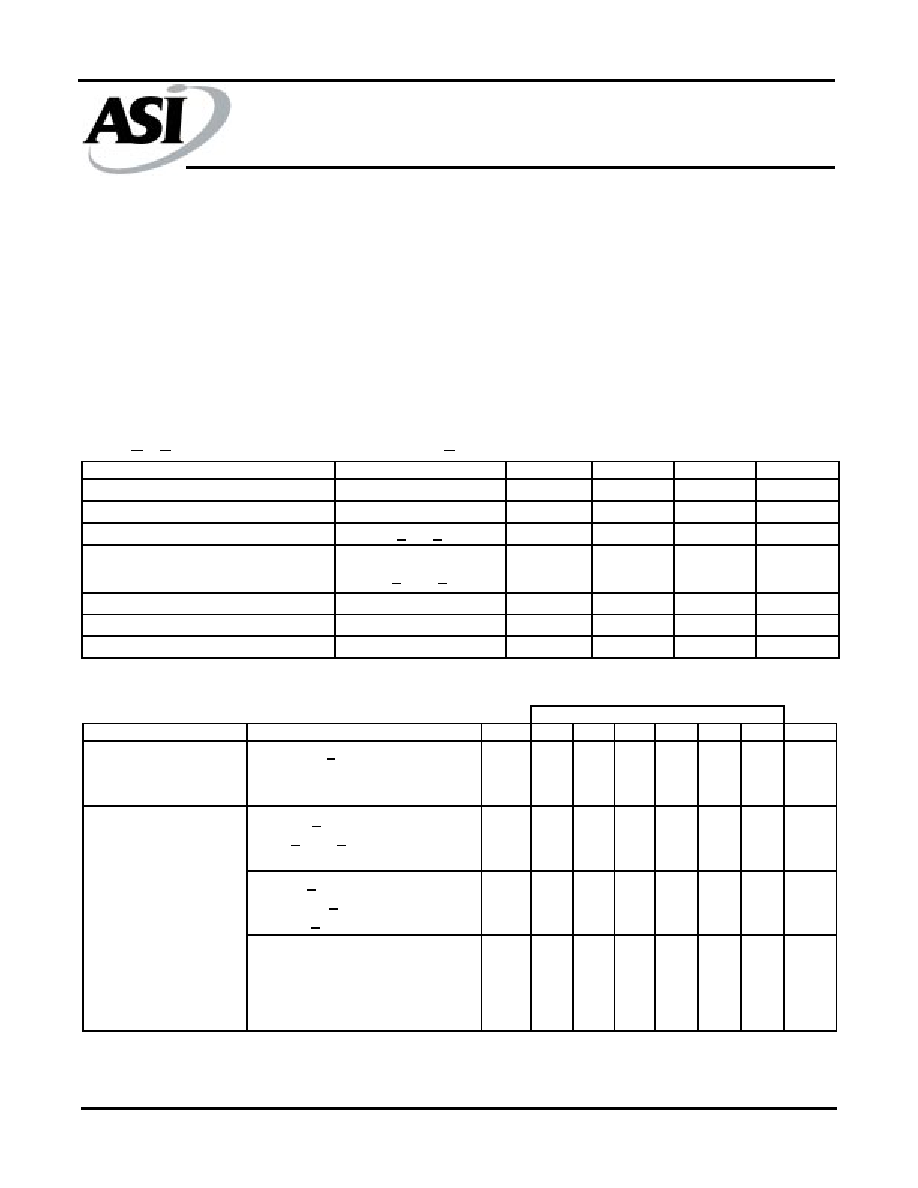
ELECTRICAL CHARACTERISTICS AND RECOMMENDED DC OPERATING CONDITIONS
(-55
o
C<T
A
<125
o
C or -40
o
C to +85
o
C; Vcc = 5V + 10%)
�
�
�
�
�
�
! �"#$#%" & ''"!
( )
)
�
( ! ! �"#$#%" & ''"!
(** +*,-.
( )
)
�
(
/ 01#
0
( �
/ 1#
0
23
0
�
�
�
�
�
!"
#"
�
$%
&'
�
(' #"
&'
$%
�
!"#)! * #
'+,'
!"#)!
- ,!.) . $%
/ 0
1#2" / 3 ""4
".5)
�
1#2" / 3 ""4
/.+63
EEPROM
AS8E128K32
Austin Semiconductor, Inc.
AS8E128K32
Rev. 5.5 9/01
Austin Semiconductor, Inc. reserves the right to change products or specifications without notice.
4
AC TEST CONDITIONS
TEST SPECIFICATIONS
Input pulse levels...........................................V
SS
to 3V
Input rise and fall times...........................................5ns
Input timing reference levels.................................1.5V
Output reference levels.........................................1.5V
Output load................................................See Figure 1
OH
OL
I
I
Current Source
Current Source
Vz = 1.5V
(Bipolar
Supply)
Device
Under
Test
Ceff = 50pf
-
+
+
NOTES:
Vz is programmable from -2V to + 7V.
I
OL
and I
OH
programmable from 0 to 16 mA.
Vz is typically the midpoint of V
OH
and V
OL
.
I
OL
and I
OH
are adjusted to simulate a typical resistive load
circuit.
TRUTH TABLE
MODE
CE
OE
WE
I/O
Read
V
IL
V
IL
V
IH
D
OUT
Write (2)
V
IL
V
IH
V
IL
D
IN
Standby/Write
V
IH
X (1)
X
High Z
Write Inhibit
X
X
V
IH
Write Inhibit
X
V
IL
X
Output Disable
X
V
IH
X
High Z
NOTE:
1. This parameter is guaranteed but not tested.
CAPACITANCE TABLE
1
(V
IN
= 0V, f = 1 MHz, T
A
= 25
o
C)
SYMBOL
PARAMETER
MAX
UNITS
C
ADD
A0 - A16 Capacitance
40
pF
C
OE
OE\ Capacitance
40
pF
C
WE,
C
CE
WE\ and CE\ Capacitance
10
pF
C
IO
I/O 0- I/O 31 Capacitance
12
pF
Figure 1
NOTES:
1. X can be V
IL
or V
IH
2. Refer to AC Programming Waveforms
EEPROM
AS8E128K32
Austin Semiconductor, Inc.
AS8E128K32
Rev. 5.5 9/01
Austin Semiconductor, Inc. reserves the right to change products or specifications without notice.
5
AC READ WAVEFORMS
(1,2,3)
NOTES
:
1. CE\ may be delayed to t
ACC
-t
CE
after the address transition without impact on t
ACC
.
2. OE\ may be delayed to t
CE
-t
OE
after the falling edge of CE\ without impact on t
CE
or by t
ACC
-t
OE
after an address change
without inpact on t
ACC
.
3. t
DF
is specified from OE\ or CE\ whichever occurs first (C
L
= 5pF).
ELECTRICAL CHARACTERISTICS AND RECOMMENDED AC OPERATING CONDITIONS
(-55
o
C < T
A
< +125
o
C or -40
o
C to +85
o
C; Vcc = 5V +10%)
MIN
MAX
MIN
MAX MIN MAX MIN MAX MIN MAX MIN MAX
Address to Output Delay
t
ACC
120
140 150 200 250 300
ns
CE\ to Output Delay
t
CE
120
140 150 200 250 300
ns
OE\ to Output Delay
t
OE
0
50
0
55 0 55 0 55 0 55 0 55 ns
CE\ or OE\ to Output Float
t
DF
55
55 55 55 55 55
ns
Output Hold from OE\, CE\ or Address,
whichever comes first
t
OH
0
0
0 0 0 0 ns
UNITS
200 250 300
DESCRIPTION
140
120 150
SYMBOL
tACC
tOH
tOE
tDF
tCE
tRC
tRC
OUTPUT VALID
ADDRESS VALID
ADDRESS
CE/
OE\
DQ
t
CE
t
OE
t
ACC
t
OH
t
DF
EEPROM
AS8E128K32
Austin Semiconductor, Inc.
AS8E128K32
Rev. 5.5 9/01
Austin Semiconductor, Inc. reserves the right to change products or specifications without notice.
6
WRITE CYCLE NO 1.
(Chip Enable Controlled)
WRITE CYCLE NO 2.
(Write Enable Controlled)
ELECTRICAL CHARACTERISTICS AND RECOMMENDED AC WRITE CHARACTERISTICS
(-55
o
C < T
A
< +125
o
C; Vcc = 5V +10%)
Symbol
Parameter
Min
Max
Units
t
W C
Write Cyce Time
10
ms
t
AS
Address Set-up Time
4
ns
t
AH
Address Hold Time
50
ns
t
DS
Data Set-up Time
50
ns
t
DH
Data Hold Time
10
ns
t
WP
Write Pulse Width
100
ns
t
BLC
Byte Load Cycle Time
150
�
s
t
WPH
Write Pulse Width High
50
ns
tDH
tDS
tWPH
tWPH
tWP
tWP
tCH
tCS
tWC
tAH
tWC
tAS
tOEH
tOES
DATA VALID
ADDRESS VALID
OE\
ADDRESS
WE\
CE\
DQ
t
OES
t
AS
t
CS
t
WP
t
DS
t
DH
t
WPH
t
CH
t
OEH
t
WC
t
AH
tDH
tDS
tWPH
tWPH
tWP
tWP
tCH
tCS
tAH
tAS
tOEH
tOES
DATA VALID
OE\
ADDRESS
CE\
WE\
DQ
t
OES
t
AS
t
CS
t
WP
t
AH
t
DS
t
DH
t
WPH
t
CH
t
OEH
EEPROM
AS8E128K32
Austin Semiconductor, Inc.
AS8E128K32
Rev. 5.5 9/01
Austin Semiconductor, Inc. reserves the right to change products or specifications without notice.
7
PAGE MODE WRITE WAVEFORMS
(1,2)
NOTES:
1. A7 through A16 must specify the page address during each high to low transition of WE\ (or CE\).
2. OE\ must be high only when WE\ and CE\ are both low.
3. VD - Valid Data
4. VA - Valid Address
PAGE MODE CHARACTERISTICS
Symbol
Parameter
Min
Max
Unit
t
AS
, t
OES
Address, OE\ Set-Up time
4
ns
t
AH
Address, Hold time
50
ns
t
CS
Chip Select Set-up Time
0
ns
t
CH
Chip Select Hold Time
0
ns
t
WP
Write Pulse Width (WE\ or CE\)
100
ns
t
DS
Data Set-up Time
50
ns
t
DH
, t
OEH
Data, OE\ Hold Time
10
ns
CHIP ERASE WAVEFORMS
t
S
= 5 msec (min.)
t
W
= tH = 10 msec (min.)
V
H
= 12.0V + 0.5V
VIH
VIL
VH
VIH
VIH
VIL
CE\
OE\
WE\
t
W
t
S
t
H
tWC
tDH
tDS
tAH
tAS
tBLC
tBLC
tWPH
tWPH
tWP
tWP
BYTE 0
BYTE 1
BYTE 2
BYTE 3
BYTE127
BYTE 126
VA
VA
VA
VA
VA
VA
VD
VD
VD
VD
VD
VD
VD
VA
VD
VD
OE
CE\
WE\
A0 - A16
DATA
t
WP
t
AH
t
AS
t
DS
t
DH
t
WPH
t
BLC
t
WC
EEPROM
AS8E128K32
Austin Semiconductor, Inc.
AS8E128K32
Rev. 5.5 9/01
Austin Semiconductor, Inc. reserves the right to change products or specifications without notice.
8
Software Data Protection Enable
Algorithm
(1)
Software Data Protection Disable
Algorithm
(1)
NOTES:
1. Data Format: I/O7 - I/O0 (Hex); Address Format: A14 - A0 (Hex)
2. Write Protect state will be active at end of write even if no other
data is loaded.
3. Write Protect state will be deactivated at end of period even if no
other data is loaded.
4. 1 to 128 bytes of data are loaded.
Load Data 55
to
Address 2AAA
Writes Enabled
(2)
Enter Data
Protect State
Load Data AA
to
Address 5555
Load Data XX
to
Any Address
(4)
Load Data A0
to
Address 5555
Load Last Byte
to
Last Address
Exit Data Protect
State
(3)
Load Data AA
to
Address 5555
Load Data 55
to
Address 2AAA
Load Data 80
to
Address 5555
Load Data AA
to
Address 5555
Load Data 20
to
Address 5555
Load Data XX
to
Any Address
(4)
Load Last Byte
to
Last Address
1. A0-A14 of the selected I/O bytes must conform to the addressing sequence for the first three bytes as shown above.
2. After the command sequence has been issued and a page write operation follows, the page address inputs (A7-A16) of the selected I/O bytes must be the same for each high to low transition
of WE\ (or CE\).
3. OE Must be high only when WE\ and CE\ are both low.
SOFTWARE PROTECTED PROGRAM CYCLE WAVEFORM
(1)(2)(3)
BYTE ADDRESS
PAGE ADDRESS
WE\
A0-A6
A7-A16
DATA
t
WC
BYTE 127
BYTE 126
BYTE 0
A0
55
AA
t
DH
t
DS
5555
2AAA
5555
t
AS
t
AH
t
BLC
t
WPH
t
WP
OE\
CE\
EEPROM
AS8E128K32
Austin Semiconductor, Inc.
AS8E128K32
Rev. 5.5 9/01
Austin Semiconductor, Inc. reserves the right to change products or specifications without notice.
9
DATA POLLING CHARACTERISTICS
(1)
NOTES:
1. Toggling either OE or CE or Both OE and CE will operate toggle bit.
2. Beginning and ending state of I/O6 will vary.
3. Any address location may be used but the address should not vary.
NOTES:
1. These parameters are characterized and not 100% tested.
2. See AC Read Characteristics.
DATA POLLING WAVEFORMS
TOGGLE BIT WAVEFORMS
(1,2,3)
NOTES:
1. These parameters are characterized and not 100% tested.
2. See AC Read Characteristics.
TOGGLE BIT CHARACTERISTICS
(1)
WE\
CE\
OE\
I/O7
A0 - A16
t
OEH
t
DH
t
OE
t
WR
High-Z
An
An
An
An
An
Symbol
Parameter
Min
Max
Units
t
DH
Data Hold Time
10
ns
t
OEH
OE\ Hold Time
10
ns
t
OE
OE\ to Output Delay
(2)
100
ns
t
W R
Write Recovery Time
0
ns
Symbol
Parameter
Min
Max
Units
t
DH
Data Hold Time
10
ns
t
OEH
OE\ Hold Time
10
ns
t
OE
OE\ to Output Delay
(2)
100
ns
t
OEPH
OE\ High Pulse
150
ns
I
CC
Write Recovery Time
0
ns
t
WR
t
OEHP
tWR
tWR
tOE
tDH
tOEH
HIGH Z
WE\
CE\
OE\
I/O 6
t
OEH
t
DH
t
OE
t
WR
t
OEHP
EEPROM
AS8E128K32
Austin Semiconductor, Inc.
AS8E128K32
Rev. 5.5 9/01
Austin Semiconductor, Inc. reserves the right to change products or specifications without notice.
10
ASI Case #703 (Package Designator Q)
SMD 5962-94585, Case Outline M
MECHANICAL DEFINITIONS*
*All measurements are in inches.
MIN
MAX
A
0.123
0.200
A1
0.000
0.020
b
0.013
0.017
B
D
D1
0.870
0.890
D2
0.980
1.000
D3
0.936
0.956
e
R
0.005
L1
0.035
0.045
SYMBOL
0.010 REF
0.050 BSC
SMD SPECIFICATIONS
0.800 BSC
4 x D2
4 x D1
4 x D
b
e
Pin 1
DETAIL A
L1
0
o
- 7
o
R
B
A1
SEE DETAIL A
A
D3
EEPROM
AS8E128K32
Austin Semiconductor, Inc.
AS8E128K32
Rev. 5.5 9/01
Austin Semiconductor, Inc. reserves the right to change products or specifications without notice.
11
MECHANICAL DEFINITIONS*
*All measurements are in inches.
ASI Case #904 (Package Designator P & PN)
SMD 5962-94585, Case Outline 4 and 5
MIN
MAX
A
0.135
0.181
A1
0.025
0.035
b
0.016
0.020
b1
0.045
0.055
b2
0.065
0.075
D
1.065
1.085
D1/E1
D2
e
L
0.132
0.155
0.600 BSC
0.100 BSC
SYMBOL
1.000 BSC
SMD SPECIFICATIONS
A
A1
L
b
e
b1
4 x D
D1
D2
E1
Pin 66
e
Pin 11
Pin 1
(identified by
0.060 square pad)
Pin 56
66 x
b2
EEPROM
AS8E128K32
Austin Semiconductor, Inc.
AS8E128K32
Rev. 5.5 9/01
Austin Semiconductor, Inc. reserves the right to change products or specifications without notice.
12
*AVAILABLE PROCESSES
IT = Industrial Temperature Range
-40
o
C to +85
o
C
XT = Extended Temperature Range
-55
o
C to +125
o
C
883C = Full Military Processing
-55
o
C to +125
o
C
PACKAGE NOTES
P = Pins 8, 21, 28, and 39 are grounds.
PN = Pins 8, 21, 28, and 39 are no connects.
ORDERING INFORMATION
Device Number
Package
Type
Speed
ns
Process
AS8E128K32
Q
-120
/*
AS8E128K32
Q
-140
/*
AS8E128K32
Q
-150
/*
AS8E128K32
Q
-200
/*
AS8E128K32
Q
-250
/*
AS8E128K32
Q
-300
/*
Device Number
Package
Type
Speed
ns
Process
AS8E128K32
AS8E128K32
P
PN
-120
-120
/*
/*
AS8E128K32
AS8E128K32
P
PN
-140
-140
/*
/*
AS8E128K32
AS8E128K32
P
PN
-150
-150
/*
/*
AS8E128K32
AS8E128K32
P
PN
-200
-200
/*
/*
AS8E128K32
AS8E128K32
P
PN
-250
-250
/*
/*
AS8E128K32
AS8E128K32
P
PN
-300
-300
/*
/*
EXAMPLE: AS8E128K32Q-250/XT
EXAMPLE: AS8E128K32P-200/883C

EEPROM
AS8E128K32
Austin Semiconductor, Inc.
AS8E128K32
Rev. 5.5 9/01
Austin Semiconductor, Inc. reserves the right to change products or specifications without notice.
13
ASI TO DSCC PART NUMBER
CROSS REFERENCE*
ASI Package Designator Q
ASI Part #
SMD Part #
AS8E128K32Q-120/883C
5962-9458506HMA
AS8E128K32Q-120/883C
5962-9458506HMC
AS8E128K32Q-140/883C
5962-9458505HMA
AS8E128K32Q-140/883C
5962-9458505HMC
AS8E128K32Q-150/883C
5962-9458504HMA
AS8E128K32Q-150/883C
5962-9458504HMC
AS8E128K32Q-200/883C
5962-9458503HMA
AS8E128K32Q-200/883C
5962-9458503HMC
AS8E128K32Q-250/883C
5962-9458502HMA
AS8E128K32Q-250/883C
5962-9458502HMC
AS8E128K32Q-300/883C
5962-9458501HMA
AS8E128K32Q-300/883C
5962-9458501HMC
ASI Package Designator P & PN
ASI Part #
SMD Part #
AS8E128K32P-120/883C
5962-9458506H5A
AS8E128K32P-120/883C
5962-9458506H5C
AS8E128K32P-140/883C
5962-9458505H5A
AS8E128K32P-140/883C
5962-9458505H5C
AS8E128K32P-150/883C
5962-9458504H5A
AS8E128K32P-150/883C
5962-9458504H5C
AS8E128K32P-200/883C
5962-9458503H5A
AS8E128K32P-200/883C
5962-9458503H5C
AS8E128K32P-250/883C
5962-9458502H5A
AS8E128K32P-250/883C
5962-9458502H5C
AS8E128K32P-300/883C
5962-9458501H5A
AS8E128K32P-300/883C
5962-9458501H5C
AS8E128K32PN-120/883C
5962-9458506H4A
AS8E128K32PN-120/883C
5962-9458506H4C
AS8E128K32PN-140/883C
5962-9458505H4A
AS8E128K32PN-140/883C
5962-9458505H4C
AS8E128K32PN-150/883C
5962-9458504H4A
AS8E128K32PN-150/883C
5962-9458504H4C
AS8E128K32PN-200/883C
5962-9458503H4A
AS8E128K32PN-200/883C
5962-9458503H4C
AS8E128K32PN-250/883C
5962-9458502H4A
AS8E128K32PN-250/883C
5962-9458502H4C
AS8E128K32PN-300/883C
5962-9458501H4A
AS8E128K32PN-300/883C
5962-9458501H4C
* ASI part number is for reference only. Orders received referencing the SMD part number will be processed per the SMD.