
EEPROM
EEPROM
EEPROM
EEPROM
EEPROM
AS8ER128K32
Austin Semiconductor, Inc.
AS8ER128K32
Rev. 4.5 2/03
Austin Semiconductor, Inc. reserves the right to change products or specifications without notice.
1
End Of Life
PLEASE NOTE:
An EOL notice was
issued on this product in 2001.
However, ASI has a large
amount of die inventory
available. For assistance,
please contact your local
sales representative.
EEPROM
EEPROM
EEPROM
EEPROM
EEPROM
AS8ER128K32
Austin Semiconductor, Inc.
AS8ER128K32
Rev. 4.5 2/03
Austin Semiconductor, Inc. reserves the right to change products or specifications without notice.
2
End Of Life
GENERAL DESCRIPTION
The Austin Semiconductor, Inc. AS8ER128K32 is a 4 Megabit
Radiation Tolerant EEPROM Module organized as 128K x 32 bit.
User configurable to 256K x16 or 512Kx 8. The module achieves high
speed access, low power consumption and high reliability by
employing advanced CMOS memory technology.
The military grade product is manufactured in compliance to
MIL-STD 883, making the AS8ER128K32 ideally suited for military
or space applications.
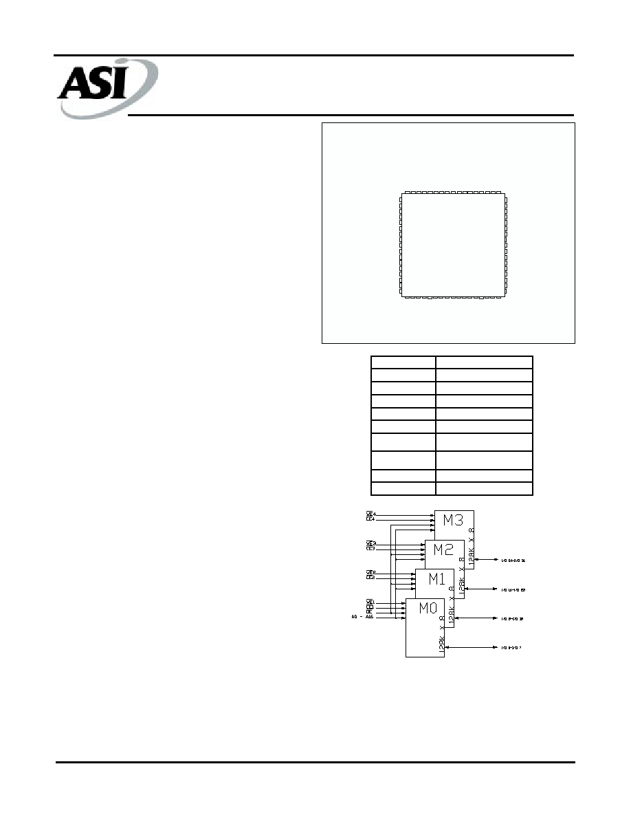
The module is offered as a 68 lead 0.990 inch square ceramic
quad flat pack. It has a max. height of 0.200 inch. This package design
is targeted for those applications which require low profile SMT
Packaging.
* contact factory for test reports. ASI does not guarantee or warrant
these performance levels, but references these third party reports.
FEATURES
�
Access time of 150ns
�
Operation with single 5V + 10% supply
�
Power Dissipation:
Active: 1.43 W (MAX), Max Speed Operation
Standby: 7.7 mW (MAX), Battery Back-up Mode
�
On-Chip Latches: Address, Data, CE\, OE\, WE\
�
Automatic Byte Write: 10 ms (MAX)
�
Automatic Page Write (128 bytes): 10 ms (MAX)
�
Data protection circuit on power on/off
�
Low power CMOS
�
10
4
Erase/Write cycles (in Page Mode)
�
Software data protection
�
TTL Compatible Inputs and Outputs
�
Data Retention: 10 years
�
Ready/Busy\ and Data Polling Signals
�
Write protection by RES\ pin
�
Radiation Tolerant: Proven total dose 40K to 100K RADS*
�
Operating Temperature Ranges:
Military: -55
o
C to +125
o
C
Industrial: -40
o
C to +85
o
C
OPTIONS
MARKINGS
�
Timing
150 ns
-150
200 ns
-200
250 ns
-250
�
Package
Ceramic Quad Flat pack
Q
No. 703
Ceramic Quad Flat pack
QB
AVAILABLE AS MILITARY
SPECIFICATIONS
�
MIL-STD-883
�
SMD 5962-94585
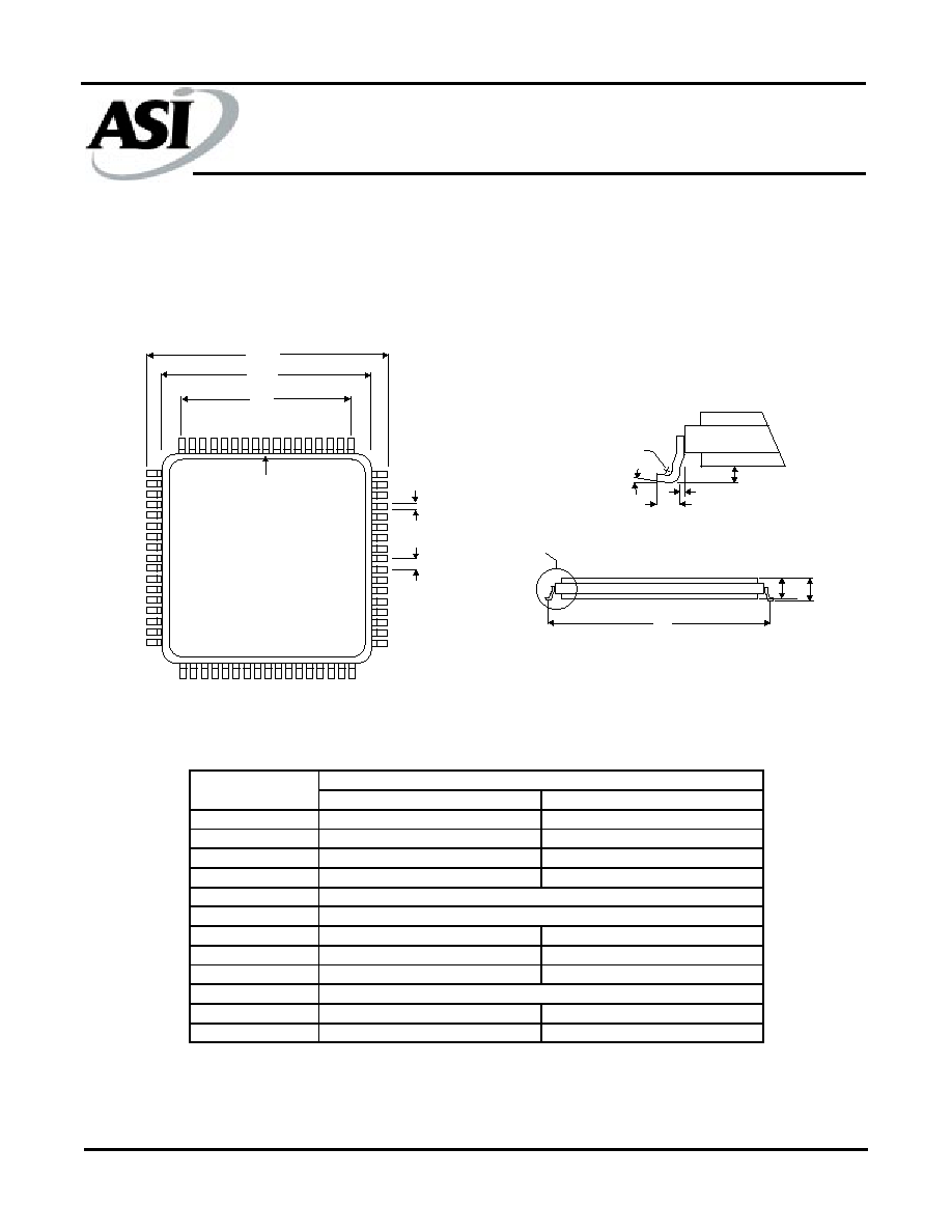
PIN ASSIGNMENT
(Top View)
68 Lead CQFP
128K x 32 EEPROM
Radiation Tolerant
EEPROM Memory Array
For more products and information
please visit our web site at
www.austinsemiconductor.com
I/O0
I/O1
I/O2
I/O3
I/O4
I/O5
I/O6
I/O7
GND
I/O8
I/O9
I/O10
I/O11
I/O12
I/O13
I/O14
I/O15
9 8 7 6 5 4 3 2 1 68 67 66 65 64 63 62 61
RES\
A0
A1
A2
A3
A4
A5
CS3\
GND
CS4\
WE1\
A6
A7
A8
A9
A10
Vcc
27 28 29 30 31 32 33 34 35 36 37 38 39 40 41 42 43
Vcc
A11
A12
A13
*A15
*A14
A16
CS1\
OE\
CS2\
NC
WE2\
WE3\
WE4\
NC
NC
RDY
10
11
12
13
14
15
16
17
18
19
20
21
22
23
24
25
26
60
59
58
57
56
55
54
53
52
51
50
49
48
47
46
45
44
I/O16
I/O17
I/O18
I/O19
I/O20
I/O21
I/O22
I/O23
GND
I/O24
I/O25
I/O26
I/O27
I/O28
I/O29
I/O30
I/O31
PIN NAME
FUNCTION
A0 to A16
Address Input
I/O0 to I/O31 Data Input/Output
OE\
Output Enable
CE\
Chip Enable
WE\
Write Enable
V
CC
Power Supply
V
SS
Ground
RDY/BUSY\
Ready Busy
RES\
Reset
FUNCTIONAL BLOCK DIAGRAM
*Pin #'s 31 and 32, A15 and A14 respectively, are reversed from the AS8E128K32. Correct
use of these address lines is required for operation of the SDP mode to work properly.
EEPROM
EEPROM
EEPROM
EEPROM
EEPROM
AS8ER128K32
Austin Semiconductor, Inc.
AS8ER128K32
Rev. 4.5 2/03
Austin Semiconductor, Inc. reserves the right to change products or specifications without notice.
3
End Of Life
NOTES:
1. RDY/Busy\ output has only active LOW V
OL
and high impedance state. It can not go to HIGH (V
OH
) state.
2. V
CC
-0.5 < V
H
< V
CC
+1.0
3. X : DON'T CARE
TRUTH TABLE
MODE
CE\
OE\
WE\
RES\
RDY/BUSY\
1
I/O
Read
V
IL
V
IL
V
IH
V
H
2
High-Z
Dout
Standby
V
IH
X
3
X
X
High-Z
High-Z
Write
V
IL
V
IH
V
IL
V
H
High-Z to V
OL
Din
Deselect
V
IL
V
IH
V
IH
V
H
High-Z
High-Z
X
X
V
IH
X
---
---
X
V
IL
X
X
---
---
Data\ Polling
V
IL
V
IL
V
IH
V
H
V
OL
Dout (I/O7)
Program Reset
X
X
X
V
IL
High-Z
High-Z
Wirte Inhibit
EEPROM
EEPROM
EEPROM
EEPROM
EEPROM
AS8ER128K32
Austin Semiconductor, Inc.
AS8ER128K32
Rev. 4.5 2/03
Austin Semiconductor, Inc. reserves the right to change products or specifications without notice.
4
End Of Life
*Stresses greater than those listed under "Absolute Maximum
Ratings" may cause permanent damage to the device. This is
a stress rating only and functional operation of the device at
these or any other conditions above those indicated in the
operation section of this specification is not implied. Exposure
to absolute maximum rating conditions for extended periods
may affect reliability.
**Junction temperature depends upon package type, cycle time,
loading, ambient temperature and airflow, and humidity
(plastics).
ABSOLUTE MAXIMUM RATINGS*
Voltage on Vcc Supply Relative to Vss
Vcc ....................................................................-0.6V to +7.0V
Operating Temperature Range
(1)
..................-55
�
C to +125
�
C
Storage Temperature Range
.........................-65
�
C to +150
�
C
Voltage on any Pin Relative to Vss..............-0.5V to +7.0V
(2)
Max Junction Temperature**.......................................+150
�
C
Thermal Resistance junction to case (
JC
):
Package Type Q...........................................11.3� C/W
Package Type P & PN..................................2.8� C/W
NOTES:
1) Including electrical characteristics and data retention.
2) V
IN
MIN = -3.0V for pulse width < 20ns.
ELECTRICAL CHARACTERISTICS AND RECOMMENDED DC OPERATING CONDITIONS
(-55
o
C<T
A
<125
o
C or -40
o
C to +85
o
C; Vcc = 5V + 10%)
MAX
CONDITIONS
SYM
-15
UNITS
Iout = 0mA, V
CC
= 5.5V
Cycle = 1�S, Duty = 100%
80
Iout = 0mA, V
CC
= 5.5V
Cycle = MIN, Duty = 100%
260
CE\ = V
CC,
V
CC
= 5.5V
I
CC1
1.4
mA
CE\ = V
IH,
V
CC
= 5.5V
I
CC2
12
mA
Power Supply Current:
Standby
I
cc3
mA
PARAMETER
Power Supply Current:
Operating
PARAMETER
CONDITIONS
SYMBOL
MIN
MAX
UNITS
Input High Voltage
V
IH
2.2
V
CC
+0.3
V
Input High Voltage (RES\)
V
H
V
CC
-0.5
V
CC
+1.0
V
Input Low Voltage
V
IL
-0.3
1
0.8
V
INPUT LEAKAGE CURRENT
OV < V
IN
< V
CC
I
LI
-10
10
�
OUTPUT LEAKAGE CURRENT
Outputs(s) Disabled,
OV < V
OUT
< V
CC
I
LO
-10
10
�
Output High Voltage
I
OH
= -0.4mA
V
OH
2.4
--
V
Output Low Voltage
I
OL
= 2.1mA
V
OL
--
0.4
V
Supply Voltage
V
CC
4.5
5.5
V
2
NOTE:
1) V
IL
(MIN): -1.0V for pulse width < 20ns.
2) I
LI
on RES\ : 500�A (MAX)
EEPROM
EEPROM
EEPROM
EEPROM
EEPROM
AS8ER128K32
Austin Semiconductor, Inc.
AS8ER128K32
Rev. 4.5 2/03
Austin Semiconductor, Inc. reserves the right to change products or specifications without notice.
5
End Of Life
NOTE:
1. This parameter is guaranteed but not tested.
CAPACITANCE TABLE
1
(V
IN
= 0V, f = 1 MHz, T
A
= 25
o
C)
SYMBOL
PARAMETER
MAX
UNITS
C
ADD
A0 - A16 Capacitance
40
pF
C
OE
OE\, RES\, RDY Capacitance
40
pF
C
WE,
C
CE
WE\ and CE\ Capacitance
12
pF
C
IO
I/O 0- I/O 31 Capacitance
20
pF
ELECTRICAL CHARACTERISTICS AND RECOMMENDED AC OPERATING CONDITIONS
(-55
o
C < T
A
< +125
o
C or -40
o
C to +85
o
C; Vcc = 5V +10%)
MIN
MAX
Address to Output Delay
CE\ = OE\ = V
IL
, WE\ = V
IH
t
ACC
150
ns
CE\ to Output Delay
OE\ = V
IL
, WE\ = V
IH
t
CE
150
ns
OE\ to Output Delay
OE\ = V
IL
, WE\ = V
IH
t
OE
10
75
ns
Address to Output Hold
CE\ = OE\ = V
IL
, WE\ = V
IH
t
OH
0
ns
CE\ or OE\ high to Output Float (1)
OE\ = V
IL
, WE\ = V
IH
t
DF
0
50
ns
RES\ low to Output Float (1)
CE\ = OE\ = V
IL
, WE\ = V
IH
t
DFR
0
350
ns
RES\ to Output Delay
CE\ = OE\ = V
IL
, WE\ = V
IH
t
RR
0
450
ns
DESCRIPTION
150
SYMBOL
UNITS
TEST CONDITIONS
AC TEST CHARACTERISTICS
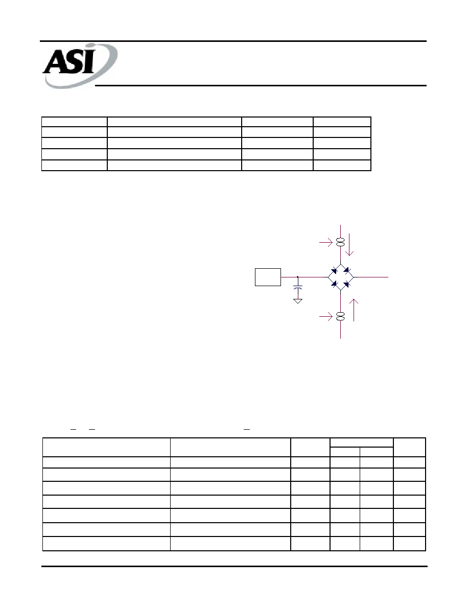
TEST SPECIFICATIONS
Input pulse levels...........................................V
SS
to 3V
Input rise and fall times...........................................5ns
Input timing reference levels.................................1.5V
Output reference levels.........................................1.5V
Output load................................................See Figure 1
OH
OL
I
I
Current Source
Current Source
Vz = 1.5V
(Bipolar
Supply)
Device
Under
Test
Ceff = 50pf
-
+
+
NOTES:
Vz is programmable from -2V to + 7V.
I
OL
and I
OH
programmable from 0 to 16 mA.
Vz is typically the midpoint of V
OH
and V
OL
.
I
OL
and I
OH
are adjusted to simulate a typical resistive load
circuit.
Figure 1
EEPROM
EEPROM
EEPROM
EEPROM
EEPROM
AS8ER128K32
Austin Semiconductor, Inc.
AS8ER128K32
Rev. 4.5 2/03
Austin Semiconductor, Inc. reserves the right to change products or specifications without notice.
6
End Of Life
ELECTRICAL CHARACTERISTICS AND RECOMMENDED AC WRITE CHARACTERISTICS
(-55
o
C < T
A
< +125
o
C; Vcc = 5V +10%)
SYMBOL
PARAMETER
MIN
(2)
MAX
UNITS
t
AS
Address Setup Time
0
ms
t
AH
Address Hold Time
150
ns
t
CS
CE\ to Write Setup Time (WE\ controlled)
0
ns
t
CH
CE\ Hold Time (WE\ controlled)
0
ns
t
WS
WE\ to Write Setup Time (CE\ controlled)
0
ns
t
WH
WE\ to Hold Time (CE\ controlled)
0
ns
t
OES
OE\ to Write Setup Time
0
ns
t
OEH
OE\ to Hold Time
0
ns
t
DS
Data Setup Time
100
ns
t
DH
Data Hold Time
10
ns
t
WP
WE\ Pulse Width (WE\ controlled)
250
ns
t
CW
CE\ Pulse Width (CE\ controlled)
250
ns
t
DL
Data Latch Time
300
ns
t
BLC
Byte Load Cycle
0.55
30
�s
t
BL
Byte Load Window
100
�s
t
WC
Write Cycle Time
10
(3)
ms
t
DB
Time to Device Busy
120
ns
t
DW
Write Start Time
150
(4)
ns
t
RP
Reset Protect Time
100
�s
t
RES
Reset High Time
(5)
1
�s
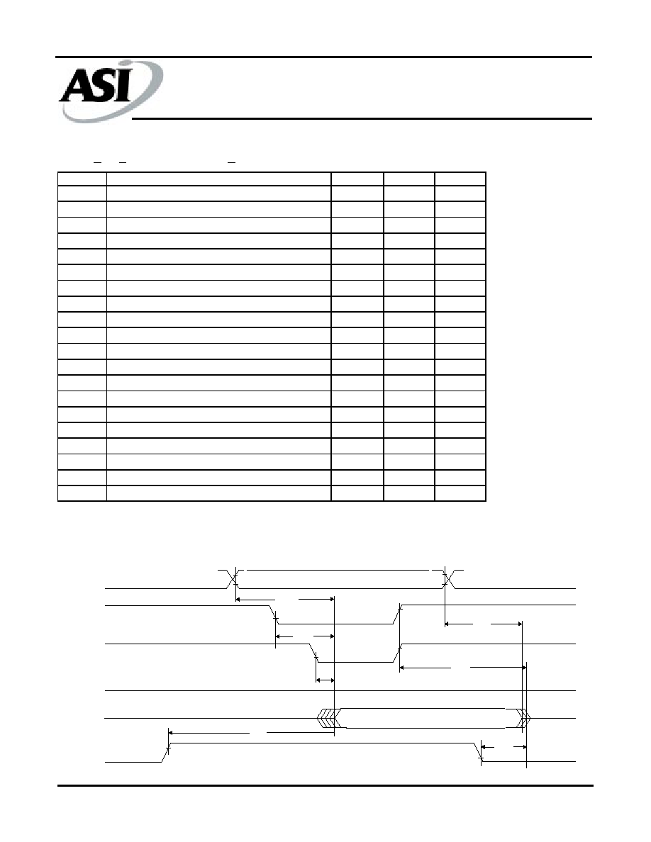
READ TIMING WAVEFORM
t
ACC
t
CE
t
OE
t
OH
t
DF
t
DFR
t
RR
HIGH-Z
ADDRESS
CE\
OE\
WE\
Data Out
RES\
DATA OUT VALID
V
IH
EEPROM
EEPROM
EEPROM
EEPROM
EEPROM
AS8ER128K32
Austin Semiconductor, Inc.
AS8ER128K32
Rev. 4.5 2/03
Austin Semiconductor, Inc. reserves the right to change products or specifications without notice.
7
End Of Life
BYTE WRITE TIMING WAVEFORM (WE\ CONTROLLED)
BYTE WRITE TIMING WAVEFORM (CE\ CONTROLLED)
t
RES
t
RP
HIGH-Z
t
OES
t
AS
t
CS
t
AH
t
WC
t
CH
t
BL
t
OEH
t
WP
t
DS
t
DH
t
DB
t
DW
HIGH-Z
V
CC
RES\
RDY/Busy\
D
in
OE\
WE\
CE\
Address
V
OL
t
RES
t
RP
HIGH-Z
t
OES
t
AS
t
WS
t
AH
t
WC
t
WH
t
BL
t
OEH
t
CW
t
DS
t
DH
t
DB
t
DW
HIGH-Z
V
CC
RES\
RDY/Busy\
D
in
OE\
WE\
CE\
Address
V
OL
EEPROM
EEPROM
EEPROM
EEPROM
EEPROM
AS8ER128K32
Austin Semiconductor, Inc.
AS8ER128K32
Rev. 4.5 2/03
Austin Semiconductor, Inc. reserves the right to change products or specifications without notice.
8
End Of Life
PAGE WRITE TIMING WAVEFORM (WE\ CONTROLLED)
PAGE WRITE TIMING WAVEFORM (CE\ CONTROLLED)
HIGH-Z
HIGH-Z
V
CC
RES\
RDY/Busy\
D
in
OE\
CE\
WE\
Address
(6)
A0 to A16
t
RES
t
RP
t
DB
t
DS
t
DH
t
OES
t
CS
t
CH
t
BLC
t
DL
t
WP
t
AS
t
AH
t
BL
t
WC
t
OEH
t
DW
HIGH-Z
HIGH-Z
V
CC
RES\
RDY/Busy\
D
in
OE\
WE\
CE\
Address
(6)
A0 to A16
t
RES
t
RP
t
DB
t
DS
t
DH
t
OES
t
WS
t
WH
t
BLC
t
DL
t
CW
t
AS
t
AH
t
BL
t
WC
t
OEH
t
DW
EEPROM
EEPROM
EEPROM
EEPROM
EEPROM
AS8ER128K32
Austin Semiconductor, Inc.
AS8ER128K32
Rev. 4.5 2/03
Austin Semiconductor, Inc. reserves the right to change products or specifications without notice.
9
End Of Life
DATA POLLING TIMING WAVEFORM
An
An
Din X
Dout X
Dout X
t
OE
(7)
t
WC
t
OEH
t
CE
(7)
t
OES
t
DW
Address
CE\
WE\
OE\
I\O7
NOTES:
1. t
DF
and t
DFR
are defined as the time at which the outputs achieve the open circuit conditions and are no longer driven.
2. Use this device in longer cycle than this value.
3. t
WC
must be longer than this value unless polling techniques or RDY/Busy\ are used. This device automatically com-
pletes the internal write operation within this value.
4. Next read or write operation can be initiated after t
DW
if polling techniques or RDY/Busy\ are used.
5. This parameter is sampled and not 100% tested.
6. A7 to A16 are page addresses and must be same within the page write operation.
7. See AC read characteristics.
EEPROM
EEPROM
EEPROM
EEPROM
EEPROM
AS8ER128K32
Austin Semiconductor, Inc.
AS8ER128K32
Rev. 4.5 2/03
Austin Semiconductor, Inc. reserves the right to change products or specifications without notice.
10
End Of Life
TOGGLE BIT
This device provides another function to determine the internal programming cycle. If the EEPROM is set to read mode
during the internal programming cycle, I/O6 will charge from "1" to "0" (toggling) for each read. When the internal pro-
gramming cycle is finished, toggling of I/O6 will stop and the device can be accessible for next read or program.
TOGGLE BIT WAVEFORM
NOTES:
1) I/O6 beginning state is "1".
2) I/O6 ending state will vary.
3) See AC read characteristics.
4) Any locations can be used, but the address must be fixed.
Dout
2
Dout
2
Dout
Dout
1
Din
t
CE
3
t
OE
3
t
OEH
t
WC
t
DW
4
Next Mode
t
OES
Address
CE\
WE\
OE\
I/O6
SOFTWARE DATA PROTECTION TIMING WAVEFORM (In protection mode)
t
WC
t
BLC
{
Address
Data (each byte)
5555
AA
AAAA or
2AAA
55
5555
A0
Write Address*
Write Data
V
CC
CE\
WE\
t
BLC
t
BLC
* During this write cycle, data is physically written to the address provided.
EEPROM
EEPROM
EEPROM
EEPROM
EEPROM
AS8ER128K32
Austin Semiconductor, Inc.
AS8ER128K32
Rev. 4.5 2/03
Austin Semiconductor, Inc. reserves the right to change products or specifications without notice.
11
End Of Life
SOFTWARE DATA PROTECTION TIMING WAVEFORM (In non-protection mode)
FUNCTIONAL DESCRIPTION
Automatic Page Write
Page-mode write feature allows 1 to 128 bytes of data to be
written into the EEPROM in a single write cycle. Following
the initial byte cycle, an additional 1 to 128 bytes can be writ-
ten in the same manner. Each additional byte load cycle must
be started within 30�s from the preceding falling edge of WE\
or CE\. When CE\ or WE\ is kept high for 100�s after data
input, the EEPROM enters write mode automatically and the
input data are written into the EEPROM.
DATA\ Polling
DATA\ polling allows the status of the EEPROM to be deter-
mined. If EEPROM is set to read mode during the write cycle,
an inversion of the last byte of data to be loaded outputs from
I/O's 7, 15, 23, and 31 to indicate that the EEPROM is per-
forming a write operation.
RDY/Busy\ Signal
RDY/Busy\ signal also allows status of the EEPROM to be
determined. The RDY/Busy\ signal has high impedance ex-
cept in write cycle and is lowered to V
OL
after the first write
signal. At the end of write cycle, the RDY/Busy\ signal changes
state to high impedance.
RES\ Signal
When RES\ is low, the EEPROM cannot be read or pro-
grammed. Therefore, data can be protected by keeping RES\
low when V
CC
is switched. RES\ should be high during read
and programming because it doesn't provide a latch function.
See timing diagram below.
Program inhibit
Program inhibit
Read inhibit
Read inhibit
V
CC
RES\
RES\ Signal Diagram
t
WC
Address
Data (each byte)
5555
AA
AAAA
or
2AAA
55
5555
80
AAAA
or
2AAA
55
V
CC
CE\
WE\
5555
AA
5555
20
Normal
active mode
EEPROM
EEPROM
EEPROM
EEPROM
EEPROM
AS8ER128K32
Austin Semiconductor, Inc.
AS8ER128K32
Rev. 4.5 2/03
Austin Semiconductor, Inc. reserves the right to change products or specifications without notice.
12
End Of Life
WE\, CE\ Pin Operation
During a write cycle, address are latched by the falling edge
of WE\ or CE\, and data is latched by the rising edge of WE\
or CE\.
Write/Erase Endurance and Data Retention Time
The endurance is 10
4
cycles in case of the page programming
and 10
3
cycles in case of the byte programming (1% cumula-
tive failure rate). The data retention time is more than 10
years when a device is page-programmed less than 10
4
cycles.
RDY/Busy\ SIGNAL
RDY/Busy\ signal also allows status of the EEPROM to
be determined. The RDY/Busy\ signal has high impedance
except in write cycle and is lowered to V
OL
after the first write
signal. At the end of the write cycle, the RDY/Busy\ signal
changes state to high impedance. This allows many 58C1001
devices RDY/Busy\ signal lines to be wired-OR together.
PROGRAMMING/ERASE
The 58C1001 does NOT employ a BULK-erase function.
The memory cells can be programmed `0' or `1'. A write cycle
performs the function of erase & write on every cycle with
the erase being transparent to the user. The internal erase data
state is considered to be `1'. To program the memory array
with background of ALL 0's or All 1's, the user would
program this data using the page mode write operation to
program all 1024 128-byte pages.
Data Protection
1. Data Protection against Noise on Control Pins (CE\,
OE\, WE\) During Operation
During readout or standby, noise on the control pins
may act as a trigger and turn the EEPROM to programming
mode by mistake. To prevent this phenomenon, this device
has a noise cancellation function that cuts noise if its width is
20ns or less in program mode.
Be careful not to allow noise of a width more than
20ns on the control pins. See Diagram 1 below.
2. Data Protection at V
CC
On/Off
When V
CC
is turned on or off, noise on the control
pins generated by external circuits (CPU, etc.) may act as a
trigger and turn the EEPROM to program mode by mistake.
To prevent this unintentional programming, the EEPROM must
be kept in an unprogrammable state while the CPR is in an
unstable state.
NOTE: The EEPROM should be kept in
unprogrammable state during V
CC
on/off by using CPU RE-
SET signal. See the timing diagram below.
DIAGRAM 1
DATA PROTECTION AT V
CC
ON/OFF
*Unprogrammable
V
CC
CPU
RESET
*Unprogrammable
EEPROM
EEPROM
EEPROM
EEPROM
EEPROM
AS8ER128K32
Austin Semiconductor, Inc.
AS8ER128K32
Rev. 4.5 2/03
Austin Semiconductor, Inc. reserves the right to change products or specifications without notice.
13
End Of Life
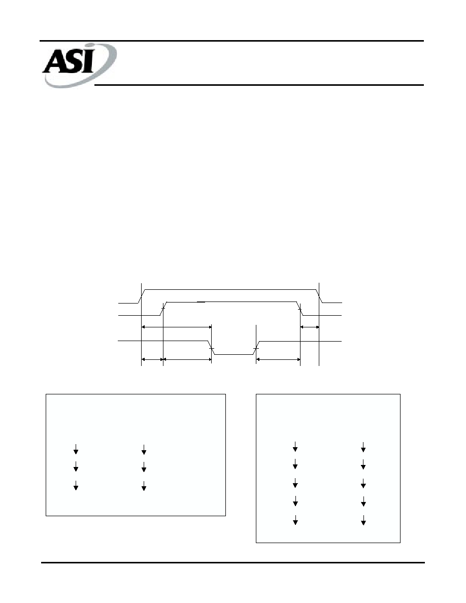
Data Protection Cont.
a. Protection by RES\
The unprogrammable state can be realized by the
CPU's reset signal inputs directly to the EEPROM's RES pin.
RES should be kept V
SS
level during V
CC
on/off.
The EEPROM brakes off programming operation
when RES becomes low, programming operation doesn't fin-
ish correctly in case that RES falls low during programming
operation. RES should be kept high for 10ms after the last
data inputs. See the timing diagram below.
3. Software data protection
To prevent unintentional programming, this device
has the software data protection (SDP) mode. The SDP is
enabled by inputting the 3 bytes code and write data in
Chart 1. SDP is not enabled if only the 3 bytes code is input.
To program data in the SDP enable mode, 3 bytes code must
be input before write data. This 4th cycle during write is
required to initiate the SDP and physically writes the address
and data. While in SDP the entire array is protected in which
writes can only occur if the exact SDP sequence is
re-executed or the unprotect sequence is executed.
The SDP is disabled by inputting the 6 bytes code in
Chart 2. Note that, if data is input in the SDP disable cycle,
data can not be written.
The software data protection is not enabled at the
shipment.
NOTE: These are some differences between ASI's
and other company's for enable/disable sequence of software
data protection. If these are any questions, please contact ASI.
PROTECTION BY RES\
Program inhibit
V
CC
RES\
Program inhibit
WE\ or CE\
1� min
100� min
10 ms min
CHART 1
Address
5555
AAAA or 2AAA
5555
Write Address
Data
(each Byte)
AA
55
A0
Write Data} Normal data input
CHART 2
Address
5555
AAAA or 2AAA
5555
5555
AAAA or 2AAA
5555
Data
(each Byte)
AA
55
80
AA
55
20
EEPROM
EEPROM
EEPROM
EEPROM
EEPROM
AS8ER128K32
Austin Semiconductor, Inc.
AS8ER128K32
Rev. 4.5 2/03
Austin Semiconductor, Inc. reserves the right to change products or specifications without notice.
14
End Of Life
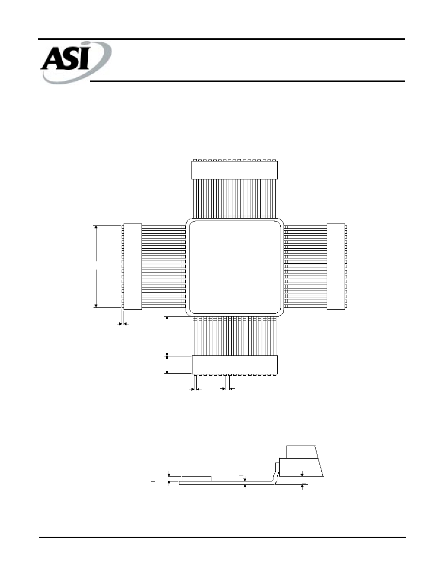
ASI Case #703 (Package Designator Q)
MECHANICAL DEFINITIONS*
*All measurements are in inches.
4 x D2
4 x D1
4 x D
b
e
Pin 1
MIN
MAX
A
0.123
0.200
A1
0.118
0.186
A2
0.000
0.020
b
0.013
0.017
B
D
D1
0.870
0.890
D2
0.980
1.000
D3
0.936
0.956
e
R
0.005
L1
0.035
0.045
SYMBOL
0.010 REF
0.050 BSC
ASI PACKAGE SPECIFICATIONS
0.800 BSC
DETAIL A
L1
0
o
- 7
o
R
B
A2
SEE DETAIL A
A
D3
A1
EEPROM
EEPROM
EEPROM
EEPROM
EEPROM
AS8ER128K32
Austin Semiconductor, Inc.
AS8ER128K32
Rev. 4.5 2/03
Austin Semiconductor, Inc. reserves the right to change products or specifications without notice.
15
End Of Life
ASI Case (Package Designator QB)
MECHANICAL DEFINITIONS*
*All measurements are in inches.
0.900
0.320
0.200
0.020
0.015
0.050
DETAIL A
0.035(+0.005)
0.008(+0.002)
0.015(+0.005)
EEPROM
EEPROM
EEPROM
EEPROM
EEPROM
AS8ER128K32
Austin Semiconductor, Inc.
AS8ER128K32
Rev. 4.5 2/03
Austin Semiconductor, Inc. reserves the right to change products or specifications without notice.
16
End Of Life
*AVAILABLE PROCESSES
IT = Industrial Temperature Range
-40
o
C to +85
o
C
XT = Extended Temperature Range
-55
o
C to +125
o
C
883C = Full Military Processing
-55
o
C to +125
o
C
ORDERING INFORMATION
Device Number
Package
Type
Speed
ns
Process
AS8ER128K32
Q
-150
/*
AS8ER128K32
Q
-200
/*
AS8ER128K32
Q
-250
/*
Device Number
Package
Type
Speed
ns
Process
AS8ER128K32
QB -150
/*
AS8ER128K32
QB -200
/*
AS8ER128K32
QB -250
/*
EXAMPLE: AS8ER128K32Q-15/IT
EXAMPLE: AS8ER128K32QB-250/XT

EEPROM
EEPROM
EEPROM
EEPROM
EEPROM
AS8ER128K32
Austin Semiconductor, Inc.
AS8ER128K32
Rev. 4.5 2/03
Austin Semiconductor, Inc. reserves the right to change products or specifications without notice.
17
End Of Life
ASI TO DSCC PART NUMBER
CROSS REFERENCE*
* ASI part number is for reference only. Orders received referencing the SMD part number will be processed per the SMD.
Package Designator Q
ASI Part #
SMD Part
AS8ER128K32Q-250/883C
5962-9458507HMX
AS8ER128K32Q-200/883C
5962-9458508HMX
AS8ER128K32Q-150/883C
5962-9458509HMX
Package Designator QB
ASI Part #
SMD Part
AS8ER128K32QB-250/883C
5962-9458507HZC
AS8ER128K32QB-200/883C
5962-9458508HZC
AS8ER128K32QB-150/883C
5962-9458509HZC