SRAM
SRAM
SRAM
SRAM
SRAM
AS8S128K32
Austin Semiconductor, Inc.
AS8S128K32
Rev. 4.0 5/03
Austin Semiconductor, Inc. reserves the right to change products or specifications without notice.
1
FEATURES
∑ Access times of 15, 17, 20, 25, 35, and 45 ns
∑ Built in decoupling caps for low noise operation
∑ Organized as 128K x32; User configured as
256Kx16 or 512K x8
∑ Operation with single 5 volt supply
∑ Low power CMOS
∑ TTL Compatible Inputs and Outputs
∑ 2V Data Retention, Low power standby
OPTIONS
MARKINGS
∑
Timing
15ns
-15
17ns
-17
20ns
-20
25ns
-25
35ns
-35
45ns
-45
∑
Package
Ceramic Quad Flatpack
Q
No. 702
Ceramic Quad Flatpack
Q1
Pin Grid Array -8 Series
P
No. 802
Pin Grid Array -8 Series
PN
No. 802
NOTE: PN indicates a no connect on pins 8, 21, 28, 39
GENERAL DESCRIPTION
The Austin Semiconductor, Inc. AS8S128K32 is a 4 Mega-
bit CMOS SRAM Module organized as 128Kx32-bits and user
configurable to 256Kx16 or 512Kx8. The AS8S128K32 achieves
high speed access, low power consumption and high reliability
by employing advanced CMOS memory technology.
The military temperature grade product is suited for mili-
tary applications.
The AS8S128K32 is offered in a ceramic quad flatpack mod-
ule per SMD-5962-95595 with a maximum height of 0.140 inches.
This module makes use of a low profile, mutlichip module de-
sign.
This device is also offered in a 1.075 inch square ceramic
pin grid array per SMD 5692-93187, which has a maximum height
of 0.195 inches. This package is also a low profile, multi-chip
module design reducing height requirements to a minimum.
AVAILABLE AS MILITARY
SPECIFICATIONS
∑ SMD 5962-95595: -Q
∑ SMD 5962-93187: -P or -PN
∑ MIL-STD-883
M3
M2
M1
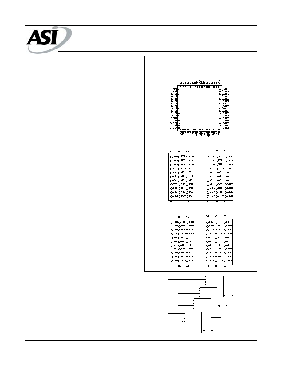
I/O 0 - I/O 7
I/O 16 - I/O 23
I/O 24 - I/O 31
I/O 8 - I/O 23
WE2
A0 - 16
OE
WE1
CE1
CE2
CE3
CE4
WE3
WE4
M0
128K x 8
128K x 8
128K x 8
128K x 8
128K x 32 SRAM
SRAM MEMORY ARRAY
PIN ASSIGNMENT
(Top View)
66 Lead PGA- Pins 8, 21, 28, 39 are no connects (PN)
66 Lead PGA- Pins 8, 21, 28, 39 are grounds (P)
68 Lead CQFP (Q & Q1)
For more products and information
please visit our web site at
www.austinsemiconductor.com

SRAM
SRAM
SRAM
SRAM
SRAM
AS8S128K32
Austin Semiconductor, Inc.
AS8S128K32
Rev. 4.0 5/03
Austin Semiconductor, Inc. reserves the right to change products or specifications without notice.
2
ABSOLUTE MAXIMUM RATINGS
*
Voltage of Vcc Supply Relative to Vss.....................-1V to +7V
Storage Temperature..........................................-65∞C to +150∞C
Short Circuit Output Current(per I/O)...............................20mA
Voltage on Any Pin Relative to Vss..................-.5V to Vcc+1V
Maximum Junction Temperature**.................................+175∞C
*Stresses greater than those listed under "Absolute Maxi-
mum Ratings" may cause permanent damage to the device.
This is a stress rating only and functional operation on the
device at these or any other conditions above those indicated
in the operational sections of this specification is not implied.
Exposure to absolute maximum rating conditions for extended
periods may affect reliability.
**Junction temperature depends upon package type, cycle time,
loading, ambient temperature and airflow. See the Application
Information section at the end of this datasheet for more infor-
mation.
ELECTRICAL CHARACTERISTICS AND RECOMMENDED DC OPERATING CONDITIONS
(-55∞C<TA<125∞C; Vcc = 5v ±10%)
�
�
�
�
�
�
�
! �"#$#%" & ''"!
( )
)
µ
! �"#$#%" & ''"!
( )
)
µ
( ! ! �"#$#%" & ''"!
(** +*,-
( )
)
µ
(
. /0#
/
( �
. 0#
/
12
/
CONDITIONS
SYM
-15
-17
-20
-25
-35
-45
UNITS NOTES
CE\<V
IL
; V
CC
=MAX
f = MAX = 1/t
RC
(MIN)
Outputs Open
I
cc
700
650
600
560
520
500
mA
3, 13
(1)
CE\>V
IH
; V
CC
=MAX
f = MAX = 1/t
RC
(MIN)
Outputs Open
I
SBT1
280
220
200
180
160
150
mA
(1)
CE\ = OE\ = V
IH
;
CMOS Compatible; V
CC
= MAX
f = 5 MHz
I
SBT2
100
80
80
60
60
60
mA
(1)
CE\ > V
cc
-0.2V; Vcc = MAX
V
IL
< V
ss
+0.2V;
V
IH
> V
CC
-0.2V; f = 0 Hz
I
SBC1
40
40
40
40
40
40
mA
(2)
CE\ > Vcc -0.2V; Vcc = MAX
V
IL
< Vss +0.2V;
V
IH
> Vcc -0.2V; f = 0 Hz
"L" Version Only
I
SBC2
24
24
24
24
24
24
mA
(2)
MAX
Power Supply Current:
Operating
PARAMETER
Power Supply Current:
Standby
NOTE:
1) Address switching sequence A, A+1, A+2, etc.
2) 1/2 input at HIGH, 1/2 input at LOW.

SRAM
SRAM
SRAM
SRAM
SRAM
AS8S128K32
Austin Semiconductor, Inc.
AS8S128K32
Rev. 4.0 5/03
Austin Semiconductor, Inc. reserves the right to change products or specifications without notice.
3
AC TEST CONDITIONS
TEST SPECIFICATIONS
Input pulse levels........................................VSS to 3V
Input rise and fall times..........................................5ns
Input timing reference levels.................................1.5V
Output reference levels........................................1.5V
Output load.............................................See Figures 1
TRUTH TABLE
MODE
OE\
CE\
WE\
I/O
POWER
Read
L
L
H
Q
ACTIVE
Write
X
L
L
D
ACTIVE
Standby
X
H
X
HIGH Z
STANDBY
Not Selected
H
L
H
HIGH Z
ACTIVE
OH
OL
I
I
Current Source
Current Source
Vz = 1.5V
(Bipolar
Supply)
Device
Under
Test
Ceff = 50pf
-
+
+
NOTES:
Vz is programable from -2V to + 7V.
I
OL
and I
OH
programmable from 0 to 16 mA.
Vz is typically the midpoint of V
OH
and V
OL
.
I
OL
and I
OH
are adjusted to simulate a typical resistive load
circuit.
SYMBOL
PARAMETER
MAX
UNITS
NOTES
C
ADD
A0 - A18 Capacitance
40
pF
4
C
OE
OE\ Capacitance
40
pF
4
C
WE,
C
CE
WE\ and CE\ Capacitance
20
pF
4
C
IO
I/O 0- I/O 31 Capacitance
20
pF
4
Figure 1
CAPACITANCE TABLE (V
IN
= 0V, f = 1 MHz, T
A
= 25
o
C)

SRAM
SRAM
SRAM
SRAM
SRAM
AS8S128K32
Austin Semiconductor, Inc.
AS8S128K32
Rev. 4.0 5/03
Austin Semiconductor, Inc. reserves the right to change products or specifications without notice.
4
ELECTRICAL CHARACTERISTICS AND RECOMMENDED AC OPERATING CONDITIONS
(Note 5) (-55
∞C
TA
125∞C; Vcc = 5v ±10%)
SYMBOL MIN MAX MIN MAX
MIN
MAX MIN MAX MIN MAX
MIN
MAX UNITS NOTES
READ CYCLE
READ cycle time
t
RC
15
17
20
25
35
45
ns
Address access time
t
AA
15
17
20
25
35
45
ns
Chip enable access time
t
ACE
15
17
20
25
35
45
ns
Output hold from address change
t
OH
2
2
2
2
2
2
ns
Chip enable to output in Low-Z
t
LZCE
2
2
2
2
2
2
ns
4, 6, 7
Chip disable to output in High-Z
t
HZCE
7
8
9
10
14
15
ns
4, 6, 7
Chip enable to power-up time
t
PU
0
0
0
0
0
0
4
Chip disable to power-down time
t
PD
15
17
20
25
35
45
4
Output enable access time
t
AOE
6
7
7
8
12
12
ns
Output enable to output in Low-Z
t
LZOE
0
0
0
0
0
0
ns
4, 6
Output disable to output in High-Z
t
HZOE
6
7
7
9
12
12
ns
4, 6, 7
WRITE CYCLE
WRITE cycle time
t
WC
15
17
20
25
35
45
ns
Chip enable to end of write
t
CW
12
12
15
17
20
22
ns
Address valid to end of write
t
AW
12
12
15
17
20
22
ns
Address setup time
t
AS
0
0
0
0
0
0
ns
Address hold from end of write
t
AH
1
1
1
1
1
1
ns
WRITE pulse width
t
WP1
12
1
12
1
15
17
20
20
ns
WRITE pulse width
t
WP2
12
1
12
1
15
17
20
20
ns
Data setup time
t
DS
8
9
10
12
15
15
ns
Data hold time
t
DH
1
1
1
1
1
1
ns
Write disable to output in Low-z
t
LZWE
2
2
2
2
2
2
ns
4, 6, 7
Write enable to output in High-Z
t
HZWE
7
9
10
11
14
15
ns
4, 6, 7
-35
-45
DESCRIPTION
-20
-25
-17
-15
NOTES:
1) For OE\ = HIGH condition. For OE\ = LOW condition
t
WP1 =
t
WP2 = 15 ns MIN.

SRAM
SRAM
SRAM
SRAM
SRAM
AS8S128K32
Austin Semiconductor, Inc.
AS8S128K32
Rev. 4.0 5/03
Austin Semiconductor, Inc. reserves the right to change products or specifications without notice.
5
7. At any given temperature and voltage condition,
t
HZCE
, is less than t
LZCE
, and t
HZWE
is less than t
LZWE
.
8.
?
W
/
E is HIGH for READ cycle.
9. Device is continuously selected. Chip enables and output
enable are held in their active state.
10. Address valid prior to or coincident with latest occurring
chip enable.
11. t
RC
= READ cycle time.
12. Chip enable (
?
C
/
E) and write enable (
?
W
/
E) can initiate and
terminate a WRITE cycle.
13. 32 bit operation
NOTES
1. All voltages referenced to V
SS
(GND).
2. -3v for pulse width <20ns.
3. I
CC
is dependent on output loading and cycle rates.
The specified value applies with the outputs
4. This parameter is sampled.
5. Test conditions as specified with output loading as
shown in Fig. 1 unless otherwise noted.
6. t
HZCE
, t
HZOE
and t
HZWE
are specified with C
L
= 5pF
as in Fig. 2. Transition is measured +/- 200 mV
typical from steady state coltage, allowing for actual
tester RC time constant.
open, and f=
H
Z.
t
RC(MIN)
1
LOW V
CC
DATA RETENTION WAVEFORM
tR
tCDR
DATA RETENTION MODE
DATA RETENTION MODE
VDR
VDR
Vcc
CE\
4.5V
4.5V
>2V
V
IH
V
IL
DATA RETENTION ELECTRICAL CHARACTERISTICS
DESCRIPTION
SYMBOL
MIN
MAX
UNITS
NOTES
V
CC
for Retention Data
V
DR
2
--
V
CE\ > V
CC
- 0.2V V
CC
= 2.0V
I
CCDR
--
6
mA
V
IN
> V
CC
- 0.2V
V
CC
= 3V
I
CCDR
--
11.6
mA
Chip Deselect to Data
Retention Time
t
CDR
0
--
ns
4
Operation Recovery Time
t
R
t
RC
ns
4, 11
Data Retention Current
CONDITIONS

SRAM
SRAM
SRAM
SRAM
SRAM
AS8S128K32
Austin Semiconductor, Inc.
AS8S128K32
Rev. 4.0 5/03
Austin Semiconductor, Inc. reserves the right to change products or specifications without notice.
6
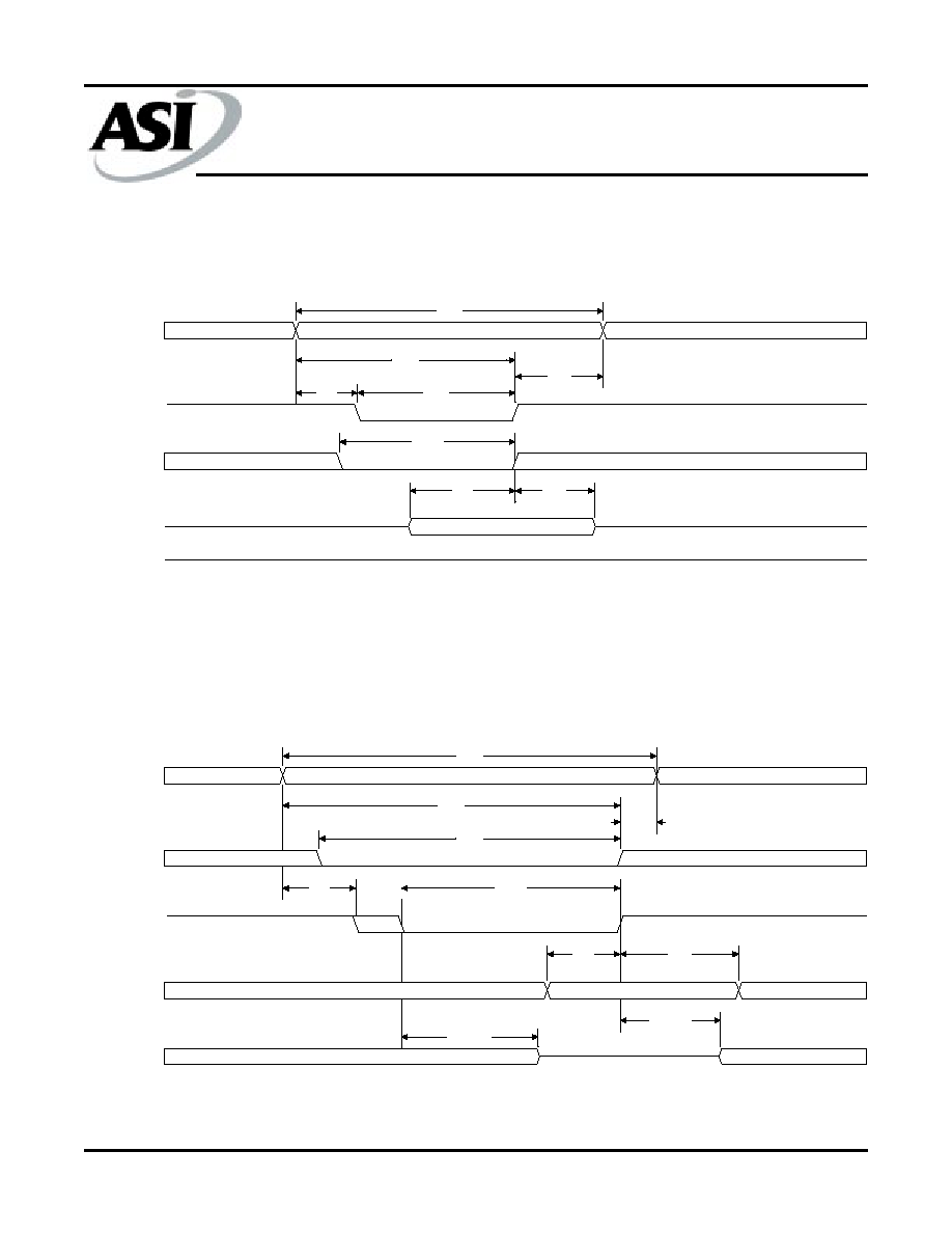
READ CYCLE NO. 2
(7,8,10)
READ CYCLE NO. 1
(8,9)
tAA
tOH
tRC
tRC
PREVIOUS DATA VALID
VALID
DATA VALID
ADDRESS
DQ
tPD
tPU
tHZCE
tACE
tLZCE
tHZOE
tLZOE
tAOE
tRC
tRC
DATA VALID
CE\
OE\
DQ
Icc
SRAM
SRAM
SRAM
SRAM
SRAM
AS8S128K32
Austin Semiconductor, Inc.
AS8S128K32
Rev. 4.0 5/03
Austin Semiconductor, Inc. reserves the right to change products or specifications without notice.
7
WRITE CYCLE NO. 1
(Chip Enable Controlled)
WRITE CYCLE NO. 2
(Write Enable Controlled)
tDH
tDS
tWP1
tWP1
tAH
tCW
tAW
tCW
tAS
tWC
tWC
HIGH Z
DATA VAILD
ADDRESS
CE\
WE\
D
Q
tLZWE
tHZWE
tDH
tDS
tWP2
tWP2
tAS
tCW
tAH
tAW
tCW
tWC
tWC
DATA VALID
ADDRESS VALID
ADDRESS
CE\
WE\
D
Q
SRAM
SRAM
SRAM
SRAM
SRAM
AS8S128K32
Austin Semiconductor, Inc.
AS8S128K32
Rev. 4.0 5/03
Austin Semiconductor, Inc. reserves the right to change products or specifications without notice.
8
MECHANICAL DEFINITIONS*
ASI Case #702 (Package Designator Q)
SMD 5962-95595, Case Outline M
*All measurements are in inches.
MIN
MAX
A
0.123
0.200
A1
0.118
0.186
A2
0.005
0.015
B
b
0.013
0.017
D
D1
0.870
0.890
D2
0.980
1.000
E
0.936
0.956
e
R
L1
0.035
0.045
0.010 TYP
SYMBOL
0.800 BSC
0.050 BSC
SMD SPECIFICATIONS
0.010 REF
A
A2
SEE DETAIL A
E3
DETAIL A
L1
1
o
- 7
o
R
B
D2
D1
D
b
e

SRAM
SRAM
SRAM
SRAM
SRAM
AS8S128K32
Austin Semiconductor, Inc.
AS8S128K32
Rev. 4.0 5/03
Austin Semiconductor, Inc. reserves the right to change products or specifications without notice.
9
MECHANICAL DEFINITIONS*
ASI Case (Package Designator Q1)
SMD 5962-95595, Case Outline A
*All measurements are in inches.
MIN
MAX
A
---
0.200
A1
0.054
---
b
0.013
0.017
B
c
0.009
0.012
D/E
0.980
1.000
D1/E1
0.870
0.890
D2/E2
e
L
0.035
0.045
R
SYMBOL
SMD SPECIFICATIONS
0.010 TYP
0.010 TYP
0.800 BSC
0.050 BSC
SRAM
SRAM
SRAM
SRAM
SRAM
AS8S128K32
Austin Semiconductor, Inc.
AS8S128K32
Rev. 4.0 5/03
Austin Semiconductor, Inc. reserves the right to change products or specifications without notice.
10
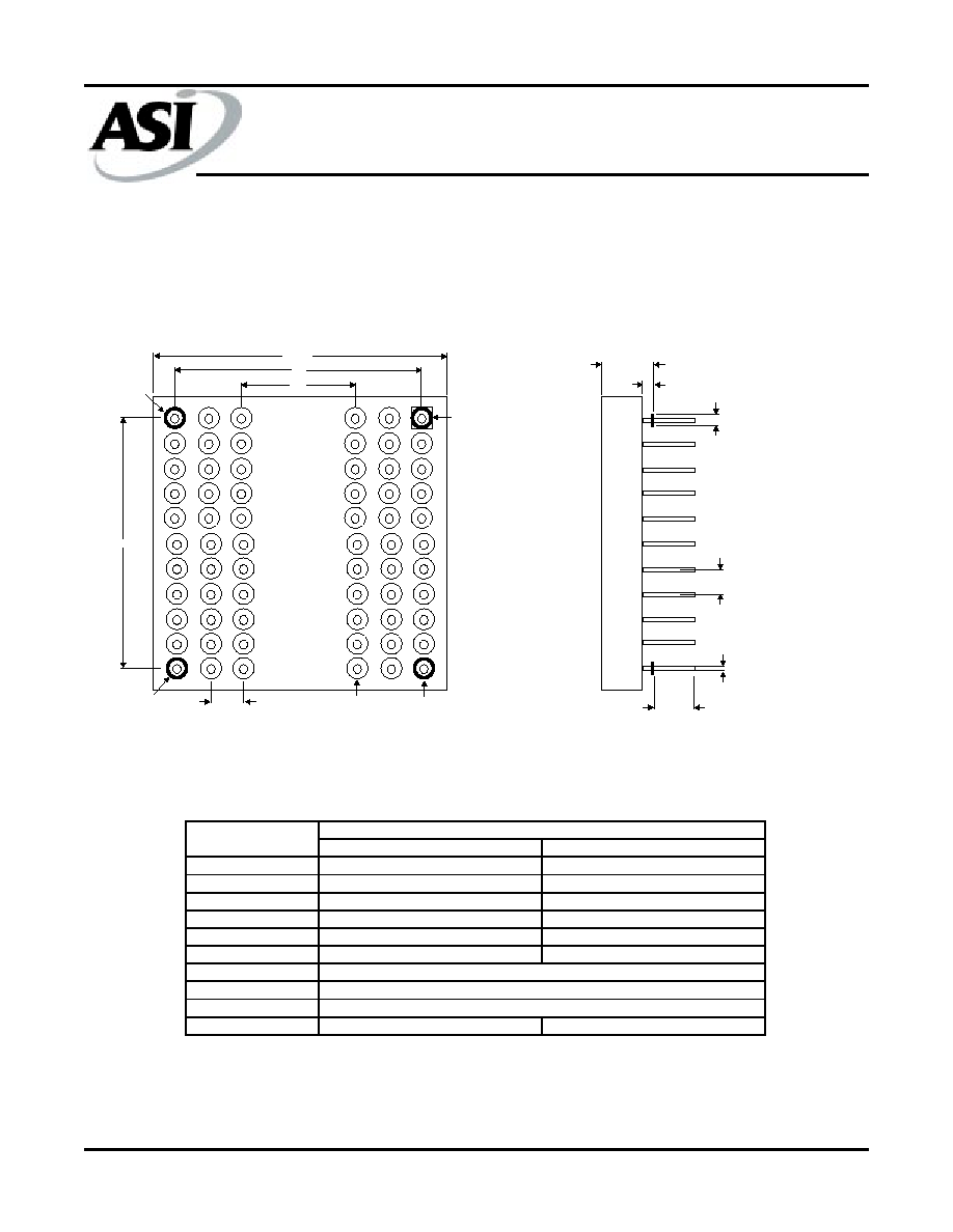
MECHANICAL DEFINITIONS*
*All measurements are in inches.
ASI Case #802 (Package Designator P & PN)
SMD 5962-93187, Case Outline 4 and 5
MIN
MAX
A
0.135
0.195
A1
0.025
0.035
b
0.016
0.020
b1
0.045
0.055
b2
0.065
0.075
D
1.064
1.086
D1/E1
D2
e
L
0.145
0.155
0.600 BSC
0.100 BSC
SYMBOL
1.000 BSC
SMD SPECIFICATIONS
A
A1
L
b
e
b1
4 x D
D1
D2
E1
Pin 66
e
Pin 11
Pin 1
(identified by
0.060 square pad)
Pin 56
b2

SRAM
SRAM
SRAM
SRAM
SRAM
AS8S128K32
Austin Semiconductor, Inc.
AS8S128K32
Rev. 4.0 5/03
Austin Semiconductor, Inc. reserves the right to change products or specifications without notice.
11
ORDERING INFORMATION
*AVAILABLE PROCESSES
IT = Industrial Temperature Range
-40
o
C to +85
o
C
XT = Extended Temperature Range
-55
o
C to +125
o
C
883C = Full Military Processing
-55
o
C to +125
o
C
PACKAGE NOTES
P = Pins 8, 21, 28, and 39 are grounds.
PN = Pins 8, 21, 28, and 39 are no connects.
Device Number
Package
Type
Speed
ns
Process
Device Number
Package
Type
Speed
ns
Process
AS8S128K32
Q
-15
/*
AS8S128K32
Q1
-15
/*
AS8S128K32
Q
-17
/*
AS8S128K32
Q1
-17
/*
AS8S128K32
Q
-20
/*
AS8S128K32
Q1
-20
/*
AS8S128K32
Q
-25
/*
AS8S128K32
Q1
-25
/*
AS8S128K32
Q
-35
/*
AS8S128K32
Q1
-35
/*
AS8S128K32
Q
-45
/*
AS8S128K32
Q1
-45
/*
Device Number
Package
Type
Speed
ns
Process
AS8S128K32
AS8S128K32
P
PN
-15
-15
/*
/*
AS8S128K32
AS8S128K32
P
PN
-17
-17
/*
/*
AS8S128K32
AS8S128K32
P
PN
-20
-20
/*
/*
AS8S128K32
AS8S128K32
P
PN
-25
-25
/*
/*
AS8S128K32
AS8S128K32
P
PN
-35
-35
/*
/*
AS8S128K32
AS8S128K32
P
PN
-45
-45
/*
/*
EXAMPLE: AS8S128K32Q-25/XT
EXAMPLE: AS8S128K32PN-20/883C
EXAMPLE: AS8S128K32Q1-15/IT

SRAM
SRAM
SRAM
SRAM
SRAM
AS8S128K32
Austin Semiconductor, Inc.
AS8S128K32
Rev. 4.0 5/03
Austin Semiconductor, Inc. reserves the right to change products or specifications without notice.
12
ASI TO DSCC PART NUMBER
CROSS REFERENCE
ASI Package Designator Q
ASI Part #
SMD Part #
AS8S128K32Q-55/883C
5962-9559505HMA
AS8S128K32Q-55/883C
5962-9559505HMC
AS8S128K32Q-45/883C
5962-9559506HMA
AS8S128K32Q-45/883C
5962-9559506HMC
AS8S128K32Q-35/883C
5962-9559507HMA
AS8S128K32Q-35/883C
5962-9559507HMC
AS8S128K32Q-25/883C
5962-9559508HMA
AS8S128K32Q-25/883C
5962-9559508HMC
AS8S128K32Q-20/883C
5962-9559509HMA
AS8S128K32Q-20/883C
5962-9559509HMC
AS8S128K32Q-17/883C
5962-9559510HMA
AS8S128K32Q-17/883C
5962-9559510HMC
ASI Part #
SMD Part #
AS8S128K32Q-55/883C
5962-9559512HMA
AS8S128K32Q-55/883C
5962-9559512HMC
AS8S128K32Q-45/883C
5962-9559513HMA
AS8S128K32Q-45/883C
5962-9559513HMC
AS8S128K32Q-35/883C
5962-9559514HMA
AS8S128K32Q-35/883C
5962-9559514HMC
AS8S128K32Q-25/883C
5962-9559515HMA
AS8S128K32Q-25/883C
5962-9559515HMC
AS8S128K32Q-20/883C
5962-9559516HMA
AS8S128K32Q-20/883C
5962-9559516HMC
AS8S128K32Q-17/883C
5962-9559517HMA
AS8S128K32Q-17/883C
5962-9559517HMC
Please note, -15 not currently available on the SMD's.
ASI Package Designator Q1
ASI Part #
SMD Part #
AS8S128K32Q1-55/883C
5962-9559505HAA
AS8S128K32Q1-55/883C
5962-9559505HAC
AS8S128K32Q1-45/883C
5962-9559506HAA
AS8S128K32Q1-45/883C
5962-9559506HAC
AS8S128K32Q1-35/883C
5962-9559507HAA
AS8S128K32Q1-35/883C
5962-9559507HAC
AS8S128K32Q1-25/883C
5962-9559508HAA
AS8S128K32Q1-25/883C
5962-9559508HAC
AS8S128K32Q1-20/883C
5962-9559509HAA
AS8S128K32Q1-20/883C
5962-9559509HAC
AS8S128K32Q1-17/883C
5962-9559510HAA
AS8S128K32Q1-17/883C
5962-9559510HAC
ASI Part #
SMD Part #
AS8S128K32Q1-55/883C
5962-9559512HAA
AS8S128K32Q1-55/883C
5962-9559512HAC
AS8S128K32Q1-45/883C
5962-9559513HAA
AS8S128K32Q1-45/883C
5962-9559513HAC
AS8S128K32Q1-35/883C
5962-9559514HAA
AS8S128K32Q1-35/883C
5962-9559514HAC
AS8S128K32Q1-25/883C
5962-9559515HAA
AS8S128K32Q1-25/883C
5962-9559515HAC
AS8S128K32Q1-20/883C
5962-9559516HAA
AS8S128K32Q1-20/883C
5962-9559516HAC
AS8S128K32Q1-17/883C
5962-9559517HAA
AS8S128K32Q1-17/883C
5962-9559517HAC
ASI Package Designator P & PN
ASI Part #
SMD Part #
AS8S128K32P-55/883C
5962-9318705H5A
AS8S128K32P-55/883C
5962-9318705H5C
AS8S128K32P-45/883C
5962-9318706H5A
AS8S128K32P-45/883C
5962-9318706H5C
AS8S128K32P-35/883C
5962-9318707H5A
AS8S128K32P-35/883C
5962-9318707H5C
AS8S128K32P-25/883C
5962-9318708H5A
AS8S128K32P-25/883C
5962-9318708H5C
AS8S128K32P-20/883C
5962-9318709H5A
AS8S128K32P-20/883C
5962-9318709H5C
AS8S128K32P-17/883C
5962-9318710H5A
AS8S128K32P-17/883C
5962-9318710H5C
ASI Part #
SMD Part #
AS8S128K32PN-55/883C
5962-9318705H4A
AS8S128K32PN-55/883C
5962-9318705H4C
AS8S128K32PN-45/883C
5962-9318706H4A
AS8S128K32PN-45/883C
5962-9318706H4C
AS8S128K32PN-35/883C
5962-9318707H4A
AS8S128K32PN-35/883C
5962-9318707H4C
AS8S128K32PN-25/883C
5962-9318708H4A
AS8S128K32PN-25/883C
5962-9318708H4C
AS8S128K32PN-20/883C
5962-9318709H4A
AS8S128K32PN-20/883C
5962-9318709H4C
AS8S128K32PN-17/883C
5962-9318710H4A
AS8S128K32PN-17/883C
5962-9318710H4C