
SRAM
MT5C1001
Limited Availability
Austin Semiconductor, Inc.
MT5C1001
Rev. 2.0 2/00
Austin Semiconductor, Inc. reserves the right to change products or specifications without notice.
1
FEATURES
∑ High Speed: 20, 25, 35, and 45
∑ Battery Backup: 2V data retention
∑ Low power standby
∑ Single +5V (+10%) Power Supply
∑ Easy memory expansion with CE\ and OE\ options.
∑ All inputs and outputs are TTL compatible
∑ Three-state output
OPTIONS
MARKING
∑ Timing
20ns access
-20
25ns access
-25
35ns access
-35
45ns access
-45
55ns access
-55*
70ns access
-70*
∑ Package(s)
Ceramic DIP (400 mil)
C
No. 109
Ceramic LCC
EC
No. 207
Ceramic Flatpack
F
No. 303
Ceramic SOJ
DCJ
No. 501
∑ Operating Temperature Ranges
Industrial (-40
o
C to +85
o
C)
IT
Military (-55
o
C to +125
o
C)
XT
∑ 2V data retention/low power
L
*Electrical characteristics identical to those provided for the
45ns access devices.
PIN ASSIGNMENT
(Top View)
AVAILABLE AS MILITARY
SPECIFICATIONS
∑ SMD 5962-92316
∑ MIL-STD-883
28-Pin DIP (C)
(400 MIL)
32-Pin LCC (EC)
32-Pin SOJ (DCJ)
32-Pin Flat Pack (F)
GENERAL DESCRIPTION
The MT5C1001 employs low power, high-performance
silicon-gate CMOS technology. Static design eliminates the
need for external clocks or timing strobes while CMOS circuitry
reduces power consumption and provides for greater
reliability.
For flexibility in high-speed memory applications, ASI
offers chip enable (CE\) and output enable (OE\) capability.
These enhancements can place the outputs in High-Z for addi-
tional flexibility in system design. Writing to these devices is
accomplished when write enable (WE|) and CE\ inputs are both
LOW. Reading is accomplished when WE\ remains HIGH while
CE\ and OE\ go LOW. The devices offer a reduced power
standby mode when disabled. This allows system designs to
achieve low standby power requirements.
The "L" version provides an approximate 50 percent
reduction in CMOS standby current (I
SBC2
) over the standard
version.
All devices operation from a single +5V power supply
and all inputs and outputs are fully TTL compatible.
1M x 1 SRAM
SRAM MEMORY ARRAY
For more products and information
please visit our web site at
www.austinsemiconductor.com
1
2
3
4
5
6
7
8
9
10
11
12
13
14
28
27
26
25
24
23
22
21
20
19
18
17
16
15
A10
A11
A12
A13
A14
A15
NC
A16
A17
A18
A19
Q
WE\
Vss
Vcc
A9
A8
A7
A6
A5
A4
NC
A3
A2
A1
A0
D
CE\
1
2
3
4
5
6
7
8
9
10
11
12
13
14
15
16
32
31
30
29
28
27
26
25
24
23
22
21
20
19
18
17
A10
A11
A12
NC
A13
A14
A15
NC
A16
A17
A18
A19
NC
Q
WE\
Vss
Vcc
NC
A9
A8
A7
A6
A5
A4
A3
NC
A2
NC
A1
A0
D
CE\
1
2
3
4
5
6
7
8
9
1 0
1 1
1 2
1 3
1 4
1 5
1 6
3 2
3 1
3 0
2 9
2 8
2 7
2 6
2 5
2 4
2 3
2 2
2 1
2 0
1 9
1 8
1 7
A10
A11
A12
NC
A13
A14
A15
NC
A16
A17
A18
A19
NC
Q
WE\
Vss
Vcc
NC
A9
A8
A7
A6
A5
A4
A3
NC
A2
NC
A1
A0
D
CE\

SRAM
MT5C1001
Limited Availability
Austin Semiconductor, Inc.
MT5C1001
Rev. 2.0 2/00
Austin Semiconductor, Inc. reserves the right to change products or specifications without notice.
2
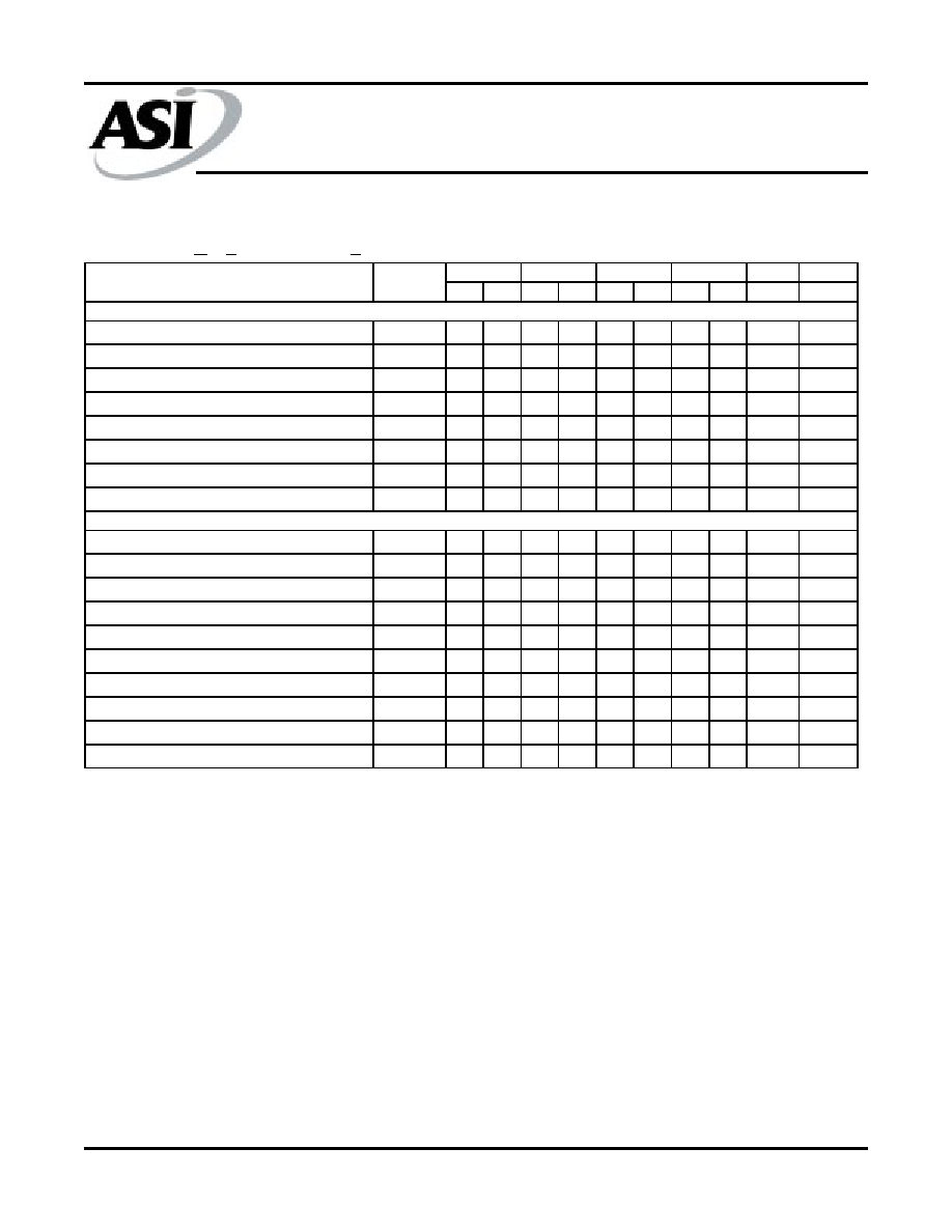
FUNCTIONAL BLOCK DIAGRAM
TRUTH TABLE
ROW DECODER
1,048,576-BIT
MEMORY ARRAY
512 rows x 2048
columns
I/O CONTROL
V
CC
Vss
D
Q
CE\
WE\
A
6
A
5
A
4
A
3
A
15
A
14
A
13
A
8
A
7
COLUMN DECODER
A
2
A
1
A
16
A
0
A
17
A
18
A
19
A
10
A
9
A
12
A
11
POWER
DOWN
MODE
CE\
WE\
OUTPUT
POWER
STANDBY
H
X
HIGH-Z
STANDBY
READ
L
H
Q
ACTIVE
WRITE
L
L
HIGH-Z
ACTIVE
PIN ASSIGNMENTS
PIN
ASSIGNMENT
A
0
-A
19
Address Inputs
WE\
Write Enable
CE\
Chip Enable
D
Data Input
Q
Data Output
NC
No Connection
V
CC
+5V Power Supply
V
SS
Ground

SRAM
MT5C1001
Limited Availability
Austin Semiconductor, Inc.
MT5C1001
Rev. 2.0 2/00
Austin Semiconductor, Inc. reserves the right to change products or specifications without notice.
3
ABSOLUTE MAXIMUM RATINGS
*
*Stresses greater than those listed under "Absolute Maximum
Ratings" may cause permanent damage to the device. This is
a stress rating only and functional operation of the device at
these or any other conditions above those indicated in the
operation section of this specification is not implied. Exposure
to absolute maximum rating conditions for extended periods
may affect reliability.
DESCRIPTION CONDITIONS
SYMBOL
MIN
MAX
UNITS
NOTES
Input High (Logic 1) Voltage
V
IH
2.2
VCC+0.5
V 1
Input Low (Logic 0) Voltage
V
IL
-0.5
0.8
V 1,
2
Input Leakage Current
0V
V
IN
VCC
IL
I
-5
5
µ
A
Output Leakage Current
Output(s) disabled
0V < V
OUT
< VCC
IL
O
-5
5
µ
A
Output High Voltage
I
OH
= -4.0mA
V
OH
2.4
V
1
Output Low Voltage
I
OL
= 8.0mA
V
OL
0.4
V
1
ELECTRICAL CHARACTERISTICS AND RECOMMENDED DC OPERATING CONDITIONS
(-55
o
C < T
C
< 125
o
C; V
CC
= 5V +10%)
CAPACITANCE
Voltage on Any Input Relative to Vss................................-.5V to +7V
Voltage on Vcc Supply Relative to Vss...............................-.5V to +7V
Voltage Applied to Q............................................................-.5V to +6V
Storage Temperature......................................................-65
o
C to +150
o
C
Power Dissipation..............................................................................1W
Short Circuit Output Current.........................................................20mA
Lead Temperature (soldering 10 seconds)....................................+260
o
C
Junction Temperature..................................................................+175
o
C
SYM
-20
-25
-35
-45
UNITS NOTES
I
cc
125
120
115
110
mA
3
Power Supply
Current: Standby
I
SBT1
50
45
40
35
mA
I
SBT2
25
25
25
25
mA
I
SBC2
10
10
10
10
mA
"L" Version Only
I
SBC2
5
5
5
5
mA
CE\ > V
CC
-0.2V; V
CC
= MAX
V
IL
< V
SS
+0.2V
V
IH
> V
CC
-0.2V; f = 0 Hz
CE\ > V
IH
; V
CC
= MAX
f = MAX = 1/t
RC
(MIN)
Output Open
CE\ > V
IH
; All Other Inputs
< V
IH
or > V
IH
, V
CC
= MAX
f = 0 Hz
MAX
CONDITIONS
CE\ < V
IL
; V
CC
= MAX
f = MAX = 1/t
RC
(MIN)
Output Open
Power Supply
Current: Operating
PARAMETER
PARAMETER CONDITIONS
SYMBOL
MAXIMUM
UNITS
NOTES
Input Capacitance (A3-A5, A15 -A17)
C
I
10 pF 4
Output Capactiance (Q)
Co
8
pF
4
Input Capacitance: (All Other Inputs) C
I
8
pF
4
T
A
= 25
o
C, f = 1MHz
V
CC
= 5V
SRAM
MT5C1001
Limited Availability
Austin Semiconductor, Inc.
MT5C1001
Rev. 2.0 2/00
Austin Semiconductor, Inc. reserves the right to change products or specifications without notice.
4
ELECTRICAL CHARACTERISTICS AND RECOMMENDED AC OPERATING CONDITIONS
(Note 5) (-55
o
C < T
C
< 125
o
C; V
CC
= 5V +10%)
MIN MAX MIN MAX MIN MAX MIN MAX UNITS NOTES
READ CYCLE
READ cycle time
t
RC
20
25
35
45
ns
Address access time
t
AA
20
25
35
45
ns
Chip Enable access time
t
ACE
20
25
35
45
ns
Output hold from address change
t
OH
3
3
3
3
ns
Chip Enable to output in Low-Z
t
LZCE
3
3
3
3
ns
4, 6, 7
Chip disable to output in High-Z
t
HZCE
8
10
15
15
ns
4, 6, 7
Chip Enable to power-up time
t
PU
0
0
0
0
ns
4
Chip disable to power-down time
t
PD
20
25
35
45
ns
4
WRITE CYCLE
WRITE cycle time
t
WC
20
25
35
45
ns
Chip Enable to end of write
t
CW
15
16
20
25
ns
Address valid to end of write
t
AW
15
16
20
25
ns
Address setup time
t
AS
0
0
0
0
ns
Address hold from end of write
t
AH
1
1
1
1
ns
WRITE pulse width
t
WP
15
16
20
25
ns
Data setup time
t
DS
8
10
13
15
ns
Data hold time
t
DH
0
0
0
0
ns
Write disable to output in Low-Z
t
LZWE
3
3
3
3
ns
7
Write Enable to output in High-Z
t
HZWE
0
9
0
10
0
13
0
13
ns
4, 6, 7
-35
-45
DESCRIPTION
-20
SYMBOL
-25
SRAM
MT5C1001
Limited Availability
Austin Semiconductor, Inc.
MT5C1001
Rev. 2.0 2/00
Austin Semiconductor, Inc. reserves the right to change products or specifications without notice.
5
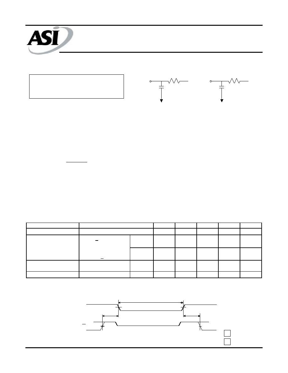
AC TEST CONDITIONS
Input pulse levels ................................... Vss to 3.0V
Input rise and fall times ....................................... 5ns
Input timing reference levels ............................. 1.5V
Output reference levels ..................................... 1.5V
Output load .............................. See Figures 1 and 2
NOTES
1.
All voltages referenced to V
SS
(GND).
2.
-3V for pulse width < 20ns
3.
I
CC
is dependent on output loading and cycle rates.
The specified value applies with the outputs
unloaded, and f = 1 Hz.
t
RC (MIN)
4.
This parameter is guaranteed but not tested.
5.
Test conditions as specified with the output loading
as shown in Fig. 1 unless otherwise noted.
6.
t
LZCE
, t
LZWE
, t
LZOE
, t
HZCE
, t
HZOE
and t
HZWE
are
specified with CL = 5pF as in Fig. 2. Transition is
measured ±200mV typical from steady state voltage,
allowing for actual tester RC time constant.
7.
At any given temperature and voltage condition,
t
HZCE
is less than t
LZCE
, and t
HZWE
is less than t
LZWE
and
t
HZOE
is less than t
LZOE
.
8.
WE\ is HIGH for READ cycle.
9.
Device is continuously selected. Chip enables and
output enables are held in their active state.
10. Address valid prior to, or coincident with, latest
occurring chip enable.
11. t
RC
= Read Cycle Time.
12. Chip enable (CE\) and write enable (WE\) can initiate and
terminate a WRITE cycle.
Fig. 1 Output Load
Equivalent
Fig. 2 Output Load
Equivalent
DATA RETENTION ELECTRICAL CHARACTERISTICS (L Version Only)
123
123
123
123
1234
1234
1234
1234
DON'T CARE
UNDEFINED
LOW Vcc DATA RETENTION WAVEFORM
V
TH
= 1.73V
Q
167
30pF
V
TH
= 1.73V
Q
167
5pF
12345678
12345678
12345678
12345678
123
123
123
123
1234
1234
1234
1234
123456789
123456789
123456789
123456789
123
123
123
123
1234
1234
1234
1234
DATA RETENTION MODE
V
DR
> 2V
4.5V
4.5V
V
DR
t
CDR
t
R
V
IH
V
IL
V
CC
CE\
DESCRIPTION SYMBOL
MIN
MAX
UNITS
NOTES
V
CC
for Retention Data
V
DR
2
--
V
V
CC
= 2V
I
CCDR
1.0 mA
V
CC
= 3V
1.5
mA
Chip Deselect to Data
Retention Time
t
CDR
0
--
ns 4
Operation Recovery Time
t
R
t
RC
ns
4, 11
Data Retention Current
CE\ > (V
CC
- 0.2V)
and
V
IN
> (V
CC
- 0.2V)
or < 0.2V
CONDITIONS
SRAM
MT5C1001
Limited Availability
Austin Semiconductor, Inc.
MT5C1001
Rev. 2.0 2/00
Austin Semiconductor, Inc. reserves the right to change products or specifications without notice.
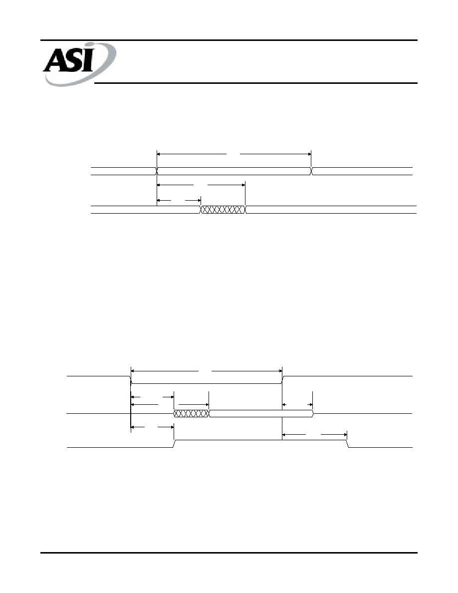
6
tAA
tOH
tRC
tRC
PREVIOUS DATA VALID
VALID
DATA VALID
ADDRESS
DQ
READ CYCLE NO. 1
8, 9
t
RC
t
AA
t
OH
tRC
tRC
CE\
READ CYCLE NO. 2
7, 8, 10
t
RC
tPD
tPU
tHZCE
tACE
tLZCE
DATA VALID
DQ
Icc
t
HZCE
t
LZCE
t
ACE
t
PU
t
PD
SRAM
MT5C1001
Limited Availability
Austin Semiconductor, Inc.
MT5C1001
Rev. 2.0 2/00
Austin Semiconductor, Inc. reserves the right to change products or specifications without notice.
7
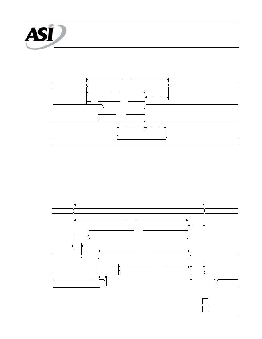
NOTE: Output enable (OE\) is inactive (HIGH).
WRITE CYCLE NO. 2
7, 12
(Write Enabled Controlled)
WRITE CYCLE NO. 1
12
(Chip Enabled Controlled)
tDH
tDS
tWP1
tWP1
tAH
tCW
tAW
tCW
tAS
tWC
tWC
HIGH Z
DATA VAILD
ADDRESS
CE\
WE\
D
Q
t
WC
t
AW
t
AS
t
CW
t
AH
t
WP
t
DS
t
DH
123456789012345678901
123456789012345678901
1
1
1
1
1
123456789012345678901234567890121234567890
123456789012345678901234567890121234567890
1
1
1
1
1
tDH
tWP1
tWP1
tAS
tAW
tCW
tAH
tCW
tWC
tWC
DATA VALID
ADDRESS
CE\
WE\
D
Q
HIGH-Z
t
DH
t
DS
t
WC
t
AW
t
AH
t
CW
t
AS
t
WP
1234
1234
1234
1234
1234567890123456
1234567890123456
1234567890123456
1234567890123456
1
1
1
1
1234
1234
1234
1234
123456
123456
123456
123456
12
12
12
12
1
1
1
1
1
1
1
1
12345678901234567
12345678901234567
12345678901234567
12
12
12
12
12
1
1
12345678901234567890123
12345678901234567890123
12345678901234567890123
12
1
1
1
1
123456789
123456789
123456789
t
HZWE
t
LZWE
123
123
123
1234
1234
1234
1234
DON'T CARE
UNDEFINED
SRAM
MT5C1001
Limited Availability
Austin Semiconductor, Inc.
MT5C1001
Rev. 2.0 2/00
Austin Semiconductor, Inc. reserves the right to change products or specifications without notice.
8
MECHANICAL DEFINITIONS*
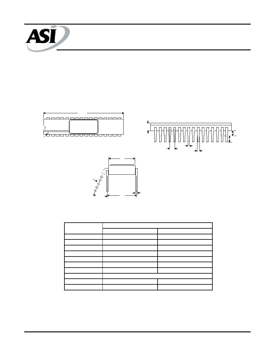
ASI Case #109 (Package Designator C)
SMD #5962-92316, Case Outline T
*All measurements are in inches.
c
NOTE
E
0
o
to 15
o
E1
D
Pin 1
e
b
b1
A
Q
L
MIN
MAX
A
0.075
0.095
b
0.016
0.020
b1
0.040
0.060
c
0.008
0.012
D
1.386
1.414
E
0.385
0.405
E1
0.390
0.410
e
L
0.125
0.175
Q
0.040
0.060
SYMBOL
SMD SPECIFICATIONS
0.100 BSC
NOTE:
These dimensions are per the SMD. ASI's package dimensional limits
may differ, but they will be within the SMD limits.

SRAM
MT5C1001
Limited Availability
Austin Semiconductor, Inc.
MT5C1001
Rev. 2.0 2/00
Austin Semiconductor, Inc. reserves the right to change products or specifications without notice.
9
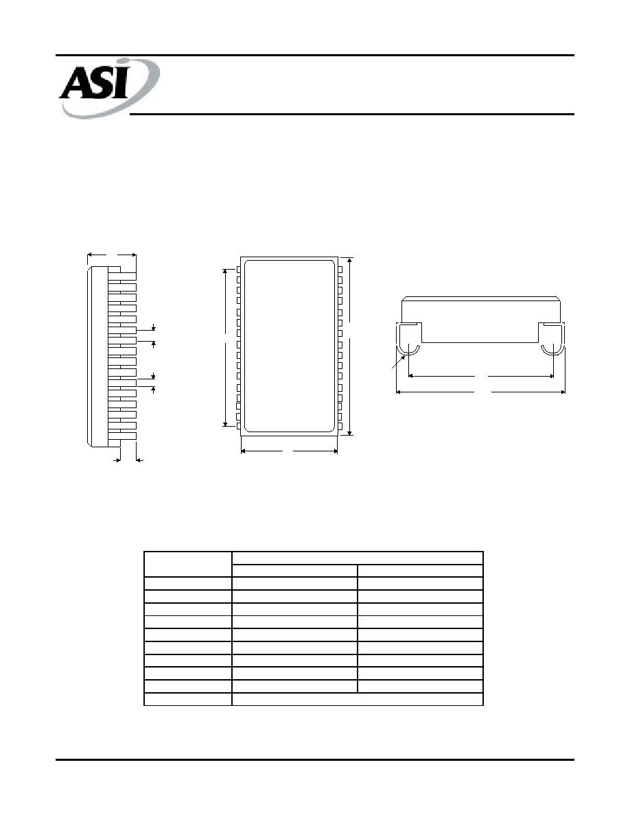
MECHANICAL DEFINITIONS*
ASI Case #207 (Package Designator EC)
SMD# 5962-92316, Case Outline Y
*All measurements are in inches.
A
b2
L1
L
e
b
b1
D1
D
E
MIN
MAX
A
0.080
0.100
b
0.022
0.028
b1
0.004
0.014
b2
0.054
0.066
D
0.815
0.835
D1
0.740
0.760
E
0.392
0.408
e
L
0.070
0.080
L1
0.090
0.110
SYMBOL
SMD SPECIFICATIONS
0.050 BSC
NOTE:
These dimensions are per the SMD. ASI's package dimensional limits
may differ, but they will be within the SMD limits.

SRAM
MT5C1001
Limited Availability
Austin Semiconductor, Inc.
MT5C1001
Rev. 2.0 2/00
Austin Semiconductor, Inc. reserves the right to change products or specifications without notice.
10
MECHANICAL DEFINITIONS*
ASI Case #303 (Package Designator F)
SMD #5962-92316, Case Outline Z
*All measurements are in inches.
Pin 1
Index
32
17
16
1
Bottom View
Top View
D
E1
L
e
b
D1
c
E
A
Q
MIN
MAX
A
0.097
0.117
b
0.015
0.019
c
0.004
0.006
D
0.812
0.828
D1
0.745
0.755
E
0.324
0.336
E1
0.405
0.415
e
L
0.290
0.310
Q
0.032
0.038
SYMBOL
SMD SPECIFICATIONS
0.050 BSC
NOTE:
These dimensions are per the SMD. ASI's package dimensional limits
may differ, but they will be within the SMD limits.
SRAM
MT5C1001
Limited Availability
Austin Semiconductor, Inc.
MT5C1001
Rev. 2.0 2/00
Austin Semiconductor, Inc. reserves the right to change products or specifications without notice.
11
*All measurements are in inches.
ASI Case #501 (Package Designator DCJ)
SMD #5962-92316, Case Outline U
MECHANICAL DEFINITIONS*
A
A2
e
b
D
E
D1
E1
E2
B1
MIN
MAX
A
0.135
0.153
A2
0.026
0.036
B1
0.030
0.040
b
0.015
0.019
D
0.812
0.828
D1
0.745
0.760
E
0.405
0.415
E1
0.435
0.445
E2
0.360
0.380
e
SYMBOL
SMD SPECIFICATIONS
0.050 BSC
NOTE:
These dimensions are per the SMD. ASI's package dimensional limits
may differ, but they will be within the SMD limits.
SRAM
MT5C1001
Limited Availability
Austin Semiconductor, Inc.
MT5C1001
Rev. 2.0 2/00
Austin Semiconductor, Inc. reserves the right to change products or specifications without notice.
12
*AVAILABLE PROCESSES
IT = Industrial Temperature Range
-40
o
C to +85
o
C
XT = Extended Temperature Range
-55
o
C to +125
o
C
883C = Full Military Processing
-55
o
C to +125
o
C
** OPTIONS
L = 2V Data Retention/Low Power
ORDERING INFORMATION
EXAMPLE:
MT5C1001EC-45/XT
Device
Number
Package
Type
Speed
ns
Options**
Process
Device
Number
Package
Type
Speed
ns
Options**
Process
MT5C1001
C
-20
L
/*
MT5C1001
EC -20
L
/*
MT5C1001
C
-25
L
/*
MT5C1001
EC -25
L
/*
MT5C1001
C
-35
L
/*
MT5C1001
EC -35
L
/*
MT5C1001
C
-40
L
/*
MT5C1001
EC -40
L
/*
MT5C1001
C
-55
L
/*
MT5C1001
EC -55
L
/*
MT5C1001
C
-70
L
/*
MT5C1001
EC -70
L
/*
EXAMPLE:
MT5C1001DCJ-70/XT
Device
Number
Package
Type
Speed
ns
Options**
Process
Device
Number
Package
Type
Speed
ns
Options**
Process
MT5C1001
F
-20
L
/*
MT5C1001
DCJ
-20
L
/*
MT5C1001
F
-25
L
/*
MT5C1001
DCJ
-25
L
/*
MT5C1001
F
-35
L
/*
MT5C1001
DCJ
-35
L
/*
MT5C1001
F
-40
L
/*
MT5C1001
DCJ
-40
L
/*
MT5C1001
F
-55
L
/*
MT5C1001
DCJ
-55
L
/*
MT5C1001
F
-70
L
/*
MT5C1001
DCJ
-70
L
/*
EXAMPLE:
MT5C1001C-20L/IT
EXAMPLE:
MT5C1001F-25L/883C

SRAM
MT5C1001
Limited Availability
Austin Semiconductor, Inc.
MT5C1001
Rev. 2.0 2/00
Austin Semiconductor, Inc. reserves the right to change products or specifications without notice.
13
ASI TO DSCC PART NUMBER
CROSS REFERENCE*
ASI Package Designator EC
ASI Part #
SMD Part #
MT5C1001EC-20L/883C
5962-9231608MYA
MT5C1001EC-20/883C
5962-9231604MYA
MT5C1001EC-25L/883C
5962-9231607MYA
MT5C1001EC-25/883C
5962-9231603MYA
MT5C1001EC-35L/883C
5962-9231606MYA
MT5C1001EC-35/883C
5962-9231602MYA
MT5C1001EC-45L/883C
5962-9231605MYA
MT5C1001EC-45/883C
5962-9231601MYA
ASI Package Designator C
ASI Part #
SMD Part #
MT5C1001C-20L/883C
5962-9231608MTA
MT5C1001C-20/883C
5962-9231604MTA
MT5C1001C-25L/883C
5962-9231607MTA
MT5C1001C-25/883C
5962-9231603MTA
MT5C1001C-35L/883C
5962-9231606MTA
MT5C1001C-35/883C
5962-9231602MTA
MT5C1001C-45L/883C
5962-9231605MTA
MT5C1001C-45/883C
5962-9231601MTA
ASI Package Designator DCJ
ASI Part #
SMD Part #
MT5C1001DCJ-20L/883C
5962-9231608MUA
MT5C1001DCJ-20/883C
5962-9231604MUA
MT5C1001DCJ-25L/883C
5962-9231607MUA
MT5C1001DCJ-25/883C
5962-9231603MUA
MT5C1001DCJ-35L/883C
5962-9231606MUA
MT5C1001DCJ-35/883C
5962-9231602MUA
MT5C1001DCJ-45L/883C
5962-9231605MUA
MT5C1001DCJ-45/883C
5962-9231601MUA
ASI Package Designator F
ASI Part #
SMD Part #
MT5C1001F-20L/883C
5962-9231608MZA
MT5C1001F-20/883C
5962-9231604MZA
MT5C1001F-25L/883C
5962-9231607MZA
MT5C1001F-25/883C
5962-9231603MZA
MT5C1001F-35L/883C
5962-9231606MZA
MT5C1001F-35/883C
5962-9231602MZA
MT5C1001F-45L/883C
5962-9231605MZA
MT5C1001F-45/883C
5962-9231601MZA
* ASI part number is for reference only. Orders received referencing the SMD part number will be processed per the SMD.