
SRAM
MT5C1009
Austin Semiconductor, Inc.
MT5C1009
Rev. 5.5 8/01
Austin Semiconductor, Inc. reserves the right to change products or specifications without notice.
1
FEATURES
∑ Access Times: 15, 20, 25, 35, 45, 55 and 70 ns
∑ Battery Backup: 2V data retention
∑ Low power standby
∑ High-performance, low-power CMOS process
∑ Single +5V (+10%) Power Supply
∑ Easy memory expansion with CE\ and OE\ options.
∑ All inputs and outputs are TTL compatible
OPTIONS
MARKING
∑ Timing
15ns access
-15
20ns access
-20
25ns access
-25
35ns access
-35
45ns access
-45
55ns access
-55*
70ns access
-70*
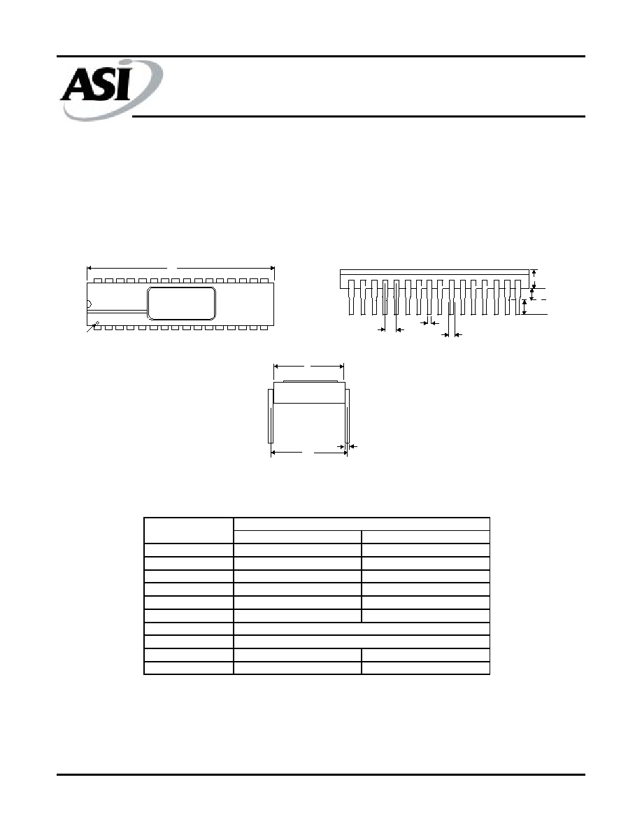
∑ Package(s)∑
Ceramic DIP (400 mil)
C
No. 111
Ceramic DIP (600 mil)
CW
No. 112
Ceramic LCC
EC
No. 207
Ceramic LCC
ECA
No. 208
Ceramic Flatpack
F
No. 303
Ceramic SOJ
DCJ
No. 501
Ceramic SOJ
SOJ
No. 507
∑ 2V data retention/low power
L
*Electrical characteristics identical to those provided for the 45ns
access devices.
PIN ASSIGNMENT
(Top View)
AVAILABLE AS MILITARY
SPECIFICATIONS
∑SMD 5962-89598
∑MIL-STD-883
NC
1
32
V
CC
A16
2
31
A15
A14
3
30
CE2
A12
4
29
WE\
A7
5
28
A13
A6
6
27
A8
A5
7
26
A9
A4
8
25
A11
A3
9
24
OE\
A2
10
23
A10
A1
11
22
CE\
A0
12
21
DQ8
DQ1
13
20
DQ7
DQ2
14
19
DQ6
DQ3
15
18
DQ5
V
SS
16
17
DQ4
NC
1
32
V
CC
A16
2
31
A15
A14
3
30
CE2
A12
4
29
WE\
A7
5
28
A13
A6
6
27
A8
A5
7
26
A9
A4
8
25
A11
A3
9
24
OE\
A2
10
23
A10
A1
11
22
CE\
A0
12
21
DQ8
DQ1
13
20
DQ7
DQ2
14
19
DQ6
DQ3
15
18
DQ5
V
SS
16
17
DQ4
NC
1
32 V
CC
A16
2
31 A15
A14
3
30 CE2
A12
4
29 WE\
A7
5
28 A13
A6
6
27 A8
A5
7
26 A9
A4
8
25 A11
A3
9
24 OE\
A2 10
23 A10
A1 11
22 CE\
A0 12
21 DQ8
DQ1 13
20 DQ7
DQ2 14
19 DQ6
DQ3 15
18 DQ5
V
SS
16
17 DQ4
32-Pin DIP (C, CW)
32-Pin SOJ (SOJ)
32-Pin LCC (EC)
32-Pin SOJ (DCJ)
32-Pin Flat Pack (F)
32-Pin LCC (ECA)
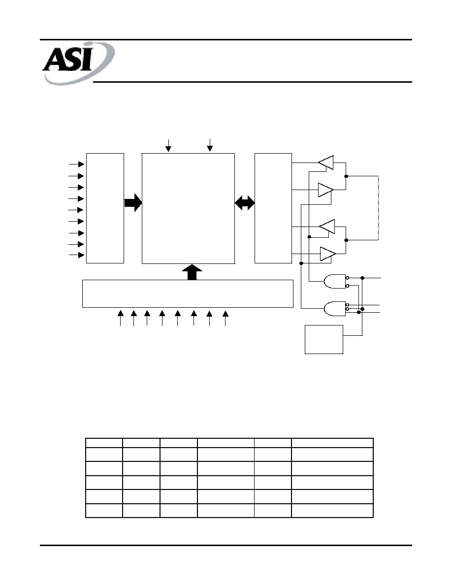
GENERAL DESCRIPTION
The MT5C1009 is a 1,048,576-bit high-speed CMOS
static RAM organized as 131,072 words by 8 bits. This device
uses 8 common input and output lines and has an output en-
able pin which operate faster than address access times during
READ cycle.
For design flexibility in high-speed memory
applications, this device offers chip enable (CE\) and output
enable (OE\) features. These enhancements can place the out-
puts in High-Z for additional flexibility in system design.
Writing to these devices is accomplished when write
enable (WE\) and CE\ inputs are both LOW. Reading is accom-
plished when WE\ remains HIGH and CE\ and OE\ go LOW.
The devices offer a reduced power standby mode when dis-
abled, allowing system designs to achieve low standby power
requirements.
The "L" version offers a 2V data retention mode, re-
ducing current consumption to 2mW maximum.
All devices operate from a single +5V power supply
and all inputs and outputs are fully TTL compatible. It is par-
ticularly well suited for use in high-density, high-speed system
applications.
128K x 8 SRAM
WITH CHIP & OUTPUT ENABLE
For more products and information
please visit our web site at
www.austinsemiconductor.com
4 3 2 1 32 31 30
A12
A14
A10
NC
V
CC
A15
CE2
14 15 16 17 18 19 20
DQ2
DQ3
V
SS
DQ4
DQ5
DQ6
DQ7
5
6
7
8
9
10
11
12
13
A7
A6
A5
A4
A3
A2
A1
A0
DQ1
29
28
27
26
25
24
23
22
21
WE
A13
A8
A9
A11
OE
A10
CE1
DQ8
\
\
\
6
NC
NC
NC
NC
SRAM
MT5C1009
Austin Semiconductor, Inc.
MT5C1009
Rev. 5.5 8/01
Austin Semiconductor, Inc. reserves the right to change products or specifications without notice.
2
FUNCTIONAL BLOCK DIAGRAM
NOTE:
The two least significant row address bits (A8 and A6) are encoded using gray code.
TRUTH TABLE
ROW DECODER
262,144-BIT
MEMORY ARRAY
I/O CONTROL
V
CC
GND
DQ8
DQ1
CE\
OE\
WE\
A
0
A
1
A
2
A
3
A
4
A
5
A
6
A
7
A
12
COLUMN DECODER
A
8
A
9
A
10
A
11
A
13
A
14
A
15
A
16
POWER
DOWN
CE\
WE\
OE\
MODE
I/O PIN
SUPPLY CURRENT
H
X
X
Not Selected
High-Z
I
SBT2
, I
SBC2
X
X
X
Not Selected
High-Z
I
SBT2
, I
SBC2
L
H
H
Output Disable
High-Z
I
CC
L
H
L
Read
D
OUT
I
CC
L
L
X
Write
D
IN
I
CC

SRAM
MT5C1009
Austin Semiconductor, Inc.
MT5C1009
Rev. 5.5 8/01
Austin Semiconductor, Inc. reserves the right to change products or specifications without notice.
3
ABSOLUTE MAXIMUM RATINGS*
Supply Voltage Range (Vcc).............................-0.5V to +6.0V
Storage Temperature......................................-65
∞
C to +150
∞
C
Short Circuit Output Current (per I/O)..........................20mA
Voltage on any Pin Relative to Vss..................-0.5V to +7.0V
Max Junction Temperature**.......................................+150
∞
C
Power Dissipation ...............................................................1 W
*Stresses at or greater than those listed under "Absolute Maxi-
mum Ratings" may cause permanent damage to the device.
This is a stress rating only and functional operation of the
device at these or any other conditions above those indicated
in the operation section of this specification is not implied.
Exposure to absolute maximum rating conditions for extended
periods will affect reliability. Refer to page 17 of this
datasheet for a technical note on this subject.
** Junction temperature depends upon package type, cycle
time, loading, ambient temperature and airflow, and humidity.
ELECTRICAL CHARACTERISTICS AND RECOMMENDED DC OPERATING CONDITIONS
(-55
o
C < T
C
< 125
o
C & -45
o
C to +85
o
C; V
CC
= 5.0V +10%)
CAPACITANCE
SYM
-15
-20
-25
-35
-45
UNITS NOTES
I
CCSP
250
140
140
135
125
mA
3
I
CCLP
250
140
130
125
115
mA
Power Supply
Current: Standby
I
SBT
25
25
25
25
25
mA
I
SBCSP
10
10
10
10
10
mA
I
SBCLP
10
10
10
10
10
mA
MAX
CONDITIONS
CE\ > V
CC
-0.2V; V
CC
= MAX
Inputs = V
IH
or V
IL
f = 0 Hz
PARAMETER
Power Supply
Current: Operating
CE\ < V
IL
; OE\ = WE\ = V
IH
,
V
CC
= MAX, f = MAX = 1/t
RC
(MIN)
Output Open
(1)
L version only
CE\ > V
IH
; All Other Inputs
< V
IL
or > V
IH
, V
CC
= MAX
f = 0 Hz
DESCRIPTION
CONDITIONS
SYM
MIN
MAX
UNITS
NOTES
Input High (Logic 1) Voltage
V
IH
2.2
V
CC
+0.5
V
1
Input Low (Logic 0) Voltage
V
IL
-0.5
0.8
V
1, 2
Input Leakage Current
0V<V
IN
<V
CC
IL
I
-10
10
µA
Output Leakage Current
Output(s) disabled
0V<V
OUT
<V
CC
IL
O
-10
10
µA
Output High Voltage
I
OH
=-4.0mA
V
OH
2.4
V
1
Output Low Voltage
I
OL
=8.0mA
V
OL
0.4
V
1
DESCRIPTION
CONDITIONS
SYM
MAX
UNITS
NOTES
Input Capacitance (A0-A16)
C
I
12
pF
4
Output Capacitance
C
O
20
pF
4
Input Capacitance (CE\, WE\, OE\)
C
I
14
pF
4
T
A
= 25
o
C, f = 1MHz
V
CC
= 5V

SRAM
MT5C1009
Austin Semiconductor, Inc.
MT5C1009
Rev. 5.5 8/01
Austin Semiconductor, Inc. reserves the right to change products or specifications without notice.
4
ELECTRICAL CHARACTERISTICS AND RECOMMENDED AC OPERATING CONDITIONS
(Note 5) (-55
o
C < T
C
< 125
o
C & -40
o
C to +85
o
C; V
CC
= 5.0V +10%)
MIN MAX MIN MAX MIN MAX MIN MAX MIN MAX UNITS NOTES
READ CYCLE
READ cycle time
t
RC
15
20
25
35
45
ns
Address access time
t
AA
15
20
25
35
45
ns
Chip Enable access time
t
ACE
15
20
25
35
45
ns
Output hold from address change
t
OH
3
3
3
3
3
ns
Chip Enable to output in Low-Z
t
LZCE
3
3
3
3
3
ns
4, 6, 7
Chip disable to output in High-Z
t
HZCE
7
8
10
15
20
ns
4, 6, 7
Output Enable access time
t
AOE
7
6
10
15
20
ns
Output Enable to output in Low-Z
t
LZOE
0
0
0
0
0
ns
4, 6, 7
Output disable to output in High-Z
t
HZOE
7
6
10
15
20
ns
4, 6, 7
WRITE CYCLE
WRITE cycle time
t
WC
15
20
25
35
45
ns
Chip Enable to end of write
t
CW
12
12
20
25
35
ns
Address valid to end of write
t
AW
12
12
20
25
35
ns
Address setup time
t
AS
0
0
0
0
0
ns
Address hold from end of write
t
AH
0
0
0
0
0
ns
WRITE pulse width (OE High)
t
WP
12
12
20
25
35
ns
Data setup time
t
DS
8
10
15
20
20
ns
Data hold time
t
DH
0
0
0
0
0
ns
Write disable to output in Low-Z
t
LZWE
5
5
5
5
5
ns
4, 6, 7
Write Enable to output in High-Z
t
HZWE
7
9
10
15
20
ns
4, 6, 7
-25
-35
-45
DESCRIPTION
-15
-20
SYMBOL
SRAM
MT5C1009
Austin Semiconductor, Inc.
MT5C1009
Rev. 5.5 8/01
Austin Semiconductor, Inc. reserves the right to change products or specifications without notice.
5
AC TEST CONDITIONS
Input pulse levels ................................... Vss to 3.0V
Input rise and fall times ....................................... 5ns
Input timing reference levels ............................. 1.5V
Output reference levels ..................................... 1.5V
Output load .............................. See Figures 1 and 2
NOTES
1.
All voltages referenced to V
SS
(GND).
2.
-2V for pulse width < 20ns
3.
I
CC
is dependent on output loading and cycle rates.
The specified value applies with the outputs
unloaded, and f = 1 Hz.
t
RC (MIN)
4.
This parameter is guaranteed but not tested.
5.
Test conditions as specified with the output loading
as shown in Fig. 1 unless otherwise noted.
6.
t
LZCE,
t
LZWE,
t
LZOE,
t
HZCE,
t
HZOE and
t
HZWE
are specified with CL = 5pF as in Fig. 2. Transition is
measured ±200mV typical from steady state voltage,
allowing for actual tester RC time constant.
7.
At any given temperature and voltage condition,
t
HZCE is less than
t
LZCE, and
t
HZWE is less than
t
LZWE and
t
HZOE is less than
t
LZOE.
8.
WE\ is HIGH for READ cycle.
9.
Device is continuously selected. Chip enables and
output enables are held in their active state.
10. Address valid prior to, or coincident with, latest
occurring chip enable.
11.
t
RC = Read Cycle Time.
Fig. 1 Output Load
Equivalent
Fig. 2 Output Load
Equivalent
DATA RETENTION ELECTRICAL CHARACTERISTICS (L Version Only)
+5V
Q
255
30
480
5 pF
+5V
Q
255
480
123
123
123
123
1234
1234
1234
1234
DON'T CARE
UNDEFINED
LOW Vcc DATA RETENTION WAVEFORM
DESCRIPTION
SYMBOL
MIN
MAX
UNITS
NOTES
V
CC
for Retention Data
V
DR
2
---
V
I
CCDR1
*
0.75
mA
I
CCDR2
1.0
mA
Chip Deselect to Data
Retention Time
t
CDR
0
---
ns
4
Operation Recovery Time
t
R
t
RC
ns
4, 11
Data Retention Current
CE\ > (V
CC
- 0.2V)
V
IN
> (V
CC
- 0.2V)
or < 0.2V
V
CC
= 2V
CONDITIONS
12345678
12345678
12345678
12345678
12345678
123
123
123
123
123
1234
1234
1234
1234
123456789
123456789
123456789
123456789
123456789
123
123
123
123
123
1234
1234
1234
1234
DATA RETENTION MODE
V
DR
> 2V
4.5V
4.5V
V
DR
t
CDR
t
R
V
IH
V
IL
V
CC
CE1\
* Low Power, -20 device only

SRAM
MT5C1009
Austin Semiconductor, Inc.
MT5C1009
Rev. 5.5 8/01
Austin Semiconductor, Inc. reserves the right to change products or specifications without notice.
6
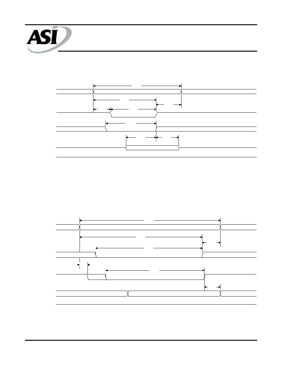
tAA
tOH
tRC
tRC
PREVIOUS DATA VALID
VALID
DATA VALID
ADDRESS
DQ
tPD
tPU
tHZCE
tACE
tLZCE
tHZOE
tLZOE
tAOE
tRC
tRC
DATA VALID
CE\
OE\
DQ
Icc
READ CYCLE NO. 1
8, 9
READ CYCLE NO. 2
7, 8, 10, 12
t
RC
t
A A
t
O H
t
RC
t
AOE
t
LZOE
t
LZCE
t
ACE
t
PU
t
HZOE
t
HZCE
t
PD
SRAM
MT5C1009
Austin Semiconductor, Inc.
MT5C1009
Rev. 5.5 8/01
Austin Semiconductor, Inc. reserves the right to change products or specifications without notice.
7
WRITE CYCLE NO. 1
12, 13
(Chip Enabled Controlled)
WRITE CYCLE NO. 2
7, 12, 13
(Write Enabled Controlled)
tDH
tDS
tWP1
tWP1
tAH
tCW
tAW
tCW
tAS
tWC
tWC
HIGH Z
DATA VAILD
ADDRESS
CE\
WE\
D
Q
tDH
tWP1
tWP1
tAS
tAW
tCW
tAH
tCW
tWC
tWC
DATA VALID
ADDRESS
CE\
WE\
D
Q
HIGH-Z
NOTE: Output enable (OE\) is inactive (HIGH).
t
WC
t
AW
t
AS
t
CW
t
A H
t
WP1
t
DS
t
D H
t
WC
t
AW
t
CW
t
AS
t
WP1
t
A H
t
D H
SRAM
MT5C1009
Austin Semiconductor, Inc.
MT5C1009
Rev. 5.5 8/01
Austin Semiconductor, Inc. reserves the right to change products or specifications without notice.
8
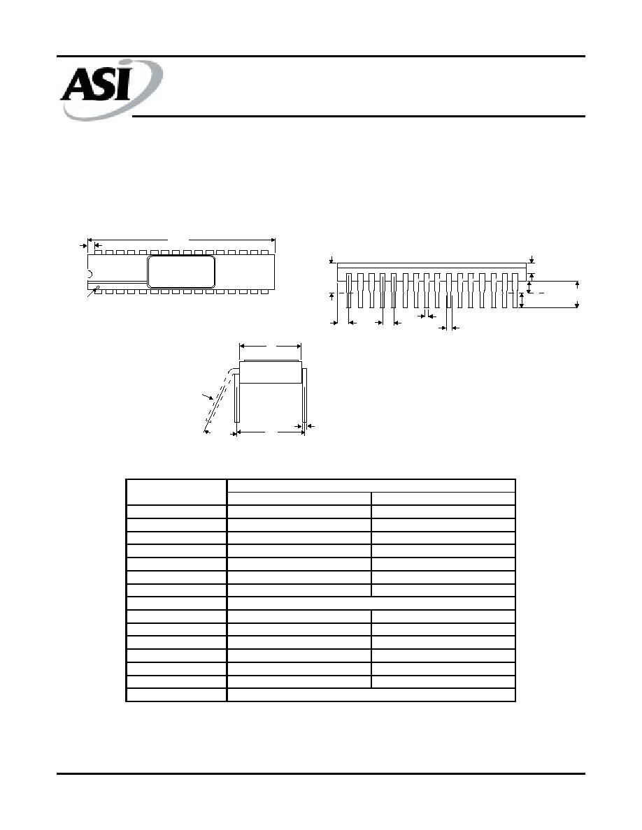
MECHANICAL DEFINITIONS*
ASI Case #111 (Package Designator C)
SMD 5962-89598, Case Outline Z
*All measurements are in inches.
D
S1
Pin 1
S
e
b
b1
A
S2
Q
L
L1
MIN
MAX
A
---
0.232
b
0.014
0.023
b1
0.038
0.065
c
0.008
0.015
D
---
1.700
E
0.350
0.405
E1
0.390
0.420
e
L
0.125
0.200
L1
0.150
---
Q
0.015
0.060
S
---
0.100
S1
0.005
---
S2
0.005
---
NOTE:
SYMBOL
0.100 BSC
SMD SPECIFICATIONS
Either configuration in detail A is allowed on SMD.
c
NOTE
E
0
o
to 15
o
E1
SRAM
MT5C1009
Austin Semiconductor, Inc.
MT5C1009
Rev. 5.5 8/01
Austin Semiconductor, Inc. reserves the right to change products or specifications without notice.
9
ASI Case #112 (Package Designator CW)
SMD 5962-89598, Case Outline X
MECHANICAL DEFINITIONS*
e
b
b2
Q
L
A
D
Pin 1
E
eA
C
*All measurements are in inches.
MIN
MAX
A
0.089
0.111
b
0.016
0.020
b2
0.045
0.050
C
0.009
0.011
D
1.585
1.615
E
0.585
0.605
eA
e
Q
0.040
0.060
L
0.125
0.175
SYMBOL
SMD Specifications
0.600 BSC
0.100 BSC

SRAM
MT5C1009
Austin Semiconductor, Inc.
MT5C1009
Rev. 5.5 8/01
Austin Semiconductor, Inc. reserves the right to change products or specifications without notice.
10
MECHANICAL DEFINITIONS*
ASI Case #207 (Package Designator EC)
SMD 5962-89598, Case Outline U
*All measurements are in inches.
b1
L2
Detail A
A
b2
MIN
MAX
A
0.080
0.100
b
0.022
0.028
b1
0.006
0.022
b2
0.040
---
D
0.800
0.840
E
0.392
0.408
e
h
L
0.070
0.080
L1
0.090
0.110
L2
0.003
0.015
SYMBOL
0.012 REF
SMD SPECIFICATIONS
0.050 BSC
D
E
See Detail A
L1
L
e
b
h x 45
o
SRAM
MT5C1009
Austin Semiconductor, Inc.
MT5C1009
Rev. 5.5 8/01
Austin Semiconductor, Inc. reserves the right to change products or specifications without notice.
11
ASI Case #208 (Package Designator ECA)
SMD 5962-89598, Case Outline M
MECHANICAL DEFINITIONS*
*All measurements are in inches.
E
D
b1
Detail A
A
b2
E1
L1
B1
D1
L
See Detail A
e
MIN
MAX
A
0.060
0.080
B1
0.022
0.028
b1
0.004
0.014
b2
0.040
0.050
D
0.442
0.458
D1
E
0.540
0.560
E1
e
L
0.045
0.055
L1
0.075
0.095
0.050 BSC
SYMBOL
SMD SPECIFICATIONS
0.300 BSC
0.400 BSC
SRAM
MT5C1009
Austin Semiconductor, Inc.
MT5C1009
Rev. 5.5 8/01
Austin Semiconductor, Inc. reserves the right to change products or specifications without notice.
12
MECHANICAL DEFINITIONS*
ASI Case #303 (Package Designator F)
SMD 5962-89598, Case Outline T
*All measurements are in inches.
c
E2
A
Q
E3
MIN
MAX
A
0.097
0.125
b
0.015
0.019
c
0.003
0.009
D
---
0.830
E
0.400
0.420
E1
---
0.450
E2
0.180
---
E3
0.030
---
e
L
0.250
0.370
Q
0.026
0.045
S
---
0.045
S1
0.000
---
SYMBOL
SMD SPECIFICATIONS
0.050 BSC
Pin 1
Index
32
17
16
1
Bottom View
D
E
L
e
b
Top View
E1
S1
S

SRAM
MT5C1009
Austin Semiconductor, Inc.
MT5C1009
Rev. 5.5 8/01
Austin Semiconductor, Inc. reserves the right to change products or specifications without notice.
13
*All measurements are in inches.
ASI Case #501 (Package Designator DCJ)
SMD 5962-89598, Case Outline 7
MECHANICAL DEFINITIONS*
MIN
MAX
A
0.135
0.144
A2
0.026
0.036
B1
0.030
0.040
b
0.015
0.019
D
0.812
0.828
D1
0.740
0.755
E
0.405
0.415
E1
0.435
0.445
E2
0.360
0.380
e
SYMBOL
SMD SPECIFICATIONS
0.050 BSC
A
A2
e
b
D
E
D1
E1
E2
B1

SRAM
MT5C1009
Austin Semiconductor, Inc.
MT5C1009
Rev. 5.5 8/01
Austin Semiconductor, Inc. reserves the right to change products or specifications without notice.
14
*All measurements are in inches.
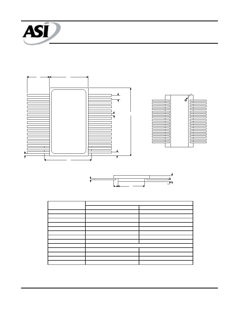
ASI Case #507 (Package Designator SOJ)
SMD 5962-89598, Case Outline Y
MECHANICAL DEFINITIONS*
S
e
A
A1
1234567890123456789012345
1234567890123456789012345
1234567890123456789012345
1234567890123456789012345
1234567890123456789012345
E2
B
B2
B1
MIN
MAX
A
0.120
0.165
A1
0.088
0.120
A2
B
B1
B2
B3
0.025
0.045
D
0.816
0.838
D1
E
0.419
0.431
E1
0.430
0.445
E2
0.360
0.380
e
e1
e2
0.005
j
S
0.030
0.040
S1
0.038 TYP
0.005 TYP
0.020 TYP
SYMBOL
SMD SPECIFICATIONS
0.050 BSC
0.070 REF
0.010 REF
.030R TYP
0.020 REF
0.75 REF
123
123
123
123
123
123
e
1
A2
e
2
S1
B3
Base
Plane
Seating
Plane
D
E
D1
j
32
1
17
16
E1
See Detail A
Detail A
SRAM
MT5C1009
Austin Semiconductor, Inc.
MT5C1009
Rev. 5.5 8/01
Austin Semiconductor, Inc. reserves the right to change products or specifications without notice.
15
*AVAILABLE PROCESSES
IT = Industrial Temperature Range
-40
o
C to +85
o
C
XT = Extended Temperature Range
-55
o
C to +125
o
C
883C = Full Military Processing
-55
o
C to +125
o
C
** OPTIONS
L = 2V data retention, low power standby
ORDERING INFORMATION
Device
Number
Package
Type
Speed
ns
Options** Process
Device
Number
Package
Type
Speed
ns
Options** Process
MT5C1009
MT5C1009
C
CW
-15
-15
L
L
/*
/*
MT5C1009
MT5C1009
EC
ECA
-15
-15
L
L
/*
/*
MT5C1009
MT5C1009
C
CW
-20
-20
L
L
/*
/*
MT5C1009
MT5C1009
EC
ECA
-20
-20
L
L
/*
/*
MT5C1009
MT5C1009
C
CW
-25
-25
L
L
/*
/*
MT5C1009
MT5C1009
EC
ECA
-25
-25
L
L
/*
/*
MT5C1009
MT5C1009
C
CW
-35
-35
L
L
/*
/*
MT5C1009
MT5C1009
EC
ECA
-35
-35
L
L
/*
/*
MT5C1009
MT5C1009
C
CW
-45
-45
L
L
/*
/*
MT5C1009
MT5C1009
EC
ECA
-45
-45
L
L
/*
/*
MT5C1009
MT5C1009
C
CW
-55
-55
L
L
/*
/*
MT5C1009
MT5C1009
EC
ECA
-55
-55
L
L
/*
/*
MT5C1009
MT5C1009
C
CW
-70
-70
L
L
/*
/*
MT5C1009
MT5C1009
EC
ECA
-70
-70
L
L
/*
/*
EXAMPLE: MT5C1009DCJ-35/883C
Device
Number
Package
Type
Speed
ns
Options** Process
Device
Number
Package
Type
Speed
ns
Options** Process
MT5C1009
F
-15
L
/*
MT5C1009
MT5C1009
DCJ
SOJ
-15
-15
L
L
/*
/*
MT5C1009
F
-20
L
/*
MT5C1009
MT5C1009
DCJ
SOJ
-20
-20
L
L
/*
/*
MT5C1009
F
-25
L
/*
MT5C1009
MT5C1009
DCJ
SOJ
-25
-25
L
L
/*
/*
MT5C1009
F
-35
L
/*
MT5C1009
MT5C1009
DCJ
SOJ
-35
-35
L
L
/*
/*
MT5C1009
F
-45
L
/*
MT5C1009
MT5C1009
DCJ
SOJ
-45
-45
L
L
/*
/*
MT5C1009
F
-55
L
/*
MT5C1009
MT5C1009
DCJ
SOJ
-55
-55
L
L
/*
/*
MT5C1009
F
-70
L
/*
MT5C1009
MT5C1009
DCJ
SOJ
-70
-70
L
L
/*
/*
EXAMPLE: MT5C1009F-70L/883C
EXAMPLE: MT5C1009C-25/XT
EXAMPLE: MT5C1009EC-45L/IT

SRAM
MT5C1009
Austin Semiconductor, Inc.
MT5C1009
Rev. 5.5 8/01
Austin Semiconductor, Inc. reserves the right to change products or specifications without notice.
16
ASI TO DSCC PART NUMBER CROSS REFERENCE
ASI Package Designator EC & ECA
ASI Part #
SMD Part #
MT5C1009EC-20/883C
5962-8959839MUA
MT5C1009EC-20L/883C
5962-8959840MUA
MT5C1009EC-25L/883C
5962-8959812MUA
MT5C1009EC-25/883C
5962-8959829MUA
MT5C1009EC-35L/883C
5962-8959811MUA
MT5C1009EC-35/883C
5962-8959828MUA
MT5C1009EC-45L/883C
5962-8959810MUA
MT5C1009EC-45/883C
5962-8959827MUA
MT5C1009EC-55L/883C
5962-8959809MUA
MT5C1009EC-55/883C
5962-8959826MUA
MT5C1009EC-70L/883C
5962-8959808MUA
MT5C1009EC-70/883C
5962-8959825MUA
MT5C1009ECA-20/883C
5962-8959839MMA
MT5C1009ECA-20L/883C
5962-8959840MMA
MT5C1009ECA-25L/883C
5962-8959812MMA
MT5C1009ECA-25/883C
5962-8959829MMA
MT5C1009ECA-35L/883C
5962-8959811MMA
MT5C1009ECA-35/883C
5962-8959828MMA
MT5C1009ECA-45L/883C
5962-8959810MMA
MT5C1009ECA-45/883C
5962-8959827MMA
MT5C1009ECA-55L/883C
5962-8959809MMA
MT5C1009ECA-55/883C
5962-8959826MMA
MT5C1009ECA-70L/883C
5962-8959808MMA
MT5C1009ECA-70/883C
5962-8959825MMA
ASI Package Designator C & CW
ASI Part #
SMD Part #
MT5C1009C-20/883C
5962-8959839MZA
MT5C1009C-20L/883C
5962-8959840MZA
MT5C1009C-25L/883C
5962-8959812MZA
MT5C1009C-25/883C
5962-8959829MZA
MT5C1009C-35L/883C
5962-8959811MZA
MT5C1009C-35/883C
5962-8959828MZA
MT5C1009C-45L/883C
5962-8959810MZA
MT5C1009C-45/883C
5962-8959827MZA
MT5C1009C-55L/883C
5962-8959809MZA
MT5C1009C-55/883C
5962-8959826MZA
MT5C1009C-70L/883C
5962-8959808MZA
MT5C1009C-70/883C
5962-8959825MZA
MT5C1009CW-20/883C
5962-8959839MXA
MT5C1009CW-20L/883C
5962-8959840MXA
MT5C1009CW-25L/883C
5962-8959812MXA
MT5C1009CW-25/883C
5962-8959829MXA
MT5C1009CW-35L/883C
5962-8959811MXA
MT5C1009CW-35/883C
5962-8959828MXA
MT5C1009CW-45L/883C
5962-8959810MXA
MT5C1009CW-45/883C
5962-8959827MXA
MT5C1009CW-55L/883C
5962-8959809MXA
MT5C1009CW-55/883C
5962-8959826MXA
MT5C1009CW-70L/883C
5962-8959808MXA
MT5C1009CW-70/883C
5962-8959825MXA
ASI Package Designator DCJ
ASI Part #
SMD Part #
MT5C1009DCJ-20/883C
5962-8959839M7A
MT5C1009DCJ-20L/883C
5962-8959840M7A
MT5C1009DCJ-25L/883C
5962-8959812M7A
MT5C1009DCJ-25/883C
5962-8959829M7A
MT5C1009DCJ-35L/883C
5962-8959811M7A
MT5C1009DCJ-35/883C
5962-8959828M7A
MT5C1009DCJ-45L/883C
5962-8959810M7A
MT5C1009DCJ-45/883C
5962-8959827M7A
MT5C1009DCJ-55L/883C
5962-8959809M7A
MT5C1009DCJ-55/883C
5962-8959826M7A
MT5C1009DCJ-70L/883C
5962-8959808M7A
MT5C1009DCJ-70/883C
5962-8959825M7A
ASI Package Designator F
ASI Part #
SMD Part #
MT5C1009F-20/883C
5962-8959839MTA
MT5C1009F-20L/883C
5962-8959840MTA
MT5C1009F-25L/883C
5962-8959812MTA
MT5C1009F-25/883C
5962-8959829MTA
MT5C1009F-35L/883C
5962-8959811MTA
MT5C1009F-35/883C
5962-8959828MTA
MT5C1009F-45L/883C
5962-8959810MTA
MT5C1009F-45/883C
5962-8959827MTA
MT5C1009F-55L/883C
5962-8959809MTA
MT5C1009F-55/883C
5962-8959826MTA
MT5C1009F-70L/883C
5962-8959808MTA
MT5C1009F-70/883C
5962-8959825MTA
* ASI part number is for reference only. Orders received referencing the SMD part number will be processed per the SMD.
ASI Package Designator SOJ
ASI Part #
SMD Part #
MT5C1009SOJ-20/883C
5962-8959839M7A
MT5C1009SOJ-20L/883C
5962-8959840M7A
MT5C1009SOJ-25L/883C
5962-8959812M7A
MT5C1009SOJ-25/883C
5962-8959829M7A
MT5C1009SOJ-35L/883C
5962-8959811M7A
MT5C1009SOJ-35/883C
5962-8959828M7A
MT5C1009SOJ-45L/883C
5962-8959810M7A
MT5C1009SOJ-45/883C
5962-8959827M7A
MT5C1009SOJ-55L/883C
5962-8959809M7A
MT5C1009SOJ-55/883C
5962-8959826M7A
MT5C1009SOJ-70L/883C
5962-8959808M7A
MT5C1009SOJ-70/883C
5962-8959825M7A

SRAM
MT5C1009
Austin Semiconductor, Inc.
MT5C1009
Rev. 5.5 8/01
Austin Semiconductor, Inc. reserves the right to change products or specifications without notice.
17
DATE: 2/6/01
Technical Note:
128Kx8 SRAM ≠ Maximum Recommended Supply
Voltage and Ambient Temperature
Compliance:
This product fully meets and is tested in compliance with SMD# 5962-89598 and tested in accordance
with JESD78.
Specific Product Affected:
Die Manufacturer: Alliance Semiconductor Corporation
Die Name: AS2008SA
Device Types: MT5C1008 , MT5C1009
Speed Grades: All
Package Designators: All
Identifying Date Code Marking: Change implemented on product starting with date code 0100.
Characteristic Identified:
Austin Semiconductor, Inc. has received notification from this die vendor, Alliance Semiconductor Corp.,
that operation at high Vcc's of 6 volts and beyond may result in a latch-up condition. This can cause
permanent damage to the device.
Recommendation:
During use in system applications and during manufacturing processes, including Burn-In and Test, the
devices should not be subjected to Vcc Supply Voltages higher than 5.5Volts at 125∞C.