SMJ28F010B
131072 BY 8-BIT
FLASH MEMORY
SGMS738 ≠ APRIL 1998
1
POST OFFICE BOX 1443
∑
HOUSTON, TEXAS 77251≠1443
D
Organization . . . 131 072
◊
8-Bit Flash
Memory
D
Pin Compatible With Existing 1M-bit
EPROMs
D
High-Reliability MIL-PRF-38535 Processing
D
V
CC
Tolerance
±
10%
D
All Inputs / Outputs TTL Compatible
D
Maximum Access / Minimum Cycle Time
28F010B-12
120 ns
'28F010B-15
150 ns
'28F010B-20
200 ns
D
Industry-Standard Programming Algorithm
D
10 000 Program / Erase-Cycle
D
Latchup Immunity of 250 mA on All Input
and Output Lines
D
Low Power Dissipation ( V
CC
= 5.5 V )
≠Active Write . . . 55 mW
≠Active Read . . . 165 mW
≠Electrical Erase . . . 82.5 mW
≠Standby . . . 0.55 mW
(CMOS-Input Levels)
D
Military Temperature Range
≠ 55
∞
C to 125
∞
C
description
The SMJ28F010B is a 104 8 576-bit, programmable read-only memory that can be electrically bulk-erased and
reprogrammed. It is available in 10 000 program / erase-endurance-cycle version.
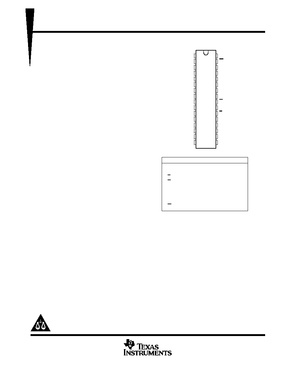
The SMJ28F010B flash memory is offered in a 32-lead ceramic 600-mil side-braze dual in-line package (DIP)
(JDD suffix) and a leadless ceramic chip carrier (FE suffix).
Please be aware that an important notice concerning availability, standard warranty, and use in critical applications of
Texas Instruments semiconductor products and disclaimers thereto appears at the end of this data sheet.
A0 ≠ A16
Address Inputs
DQ0 ≠ DQ7
Inputs (programming) / Outputs
E
Chip Enable
G
Output Enable
NC
No Internal Connection
VCC
5-V Power Supply
VPP
12-V Power Supply
V
SS
Ground
W
Write Enable
PIN NOMENCLATURE
JDD or FE PACKAGE
( TOP VIEW )
1
2
3
4
5
6
7
8
9
10
11
12
13
14
15
16
32
31
30
29
28
27
26
25
24
23
22
21
20
19
18
17
V
PP
A16
A15
A12
A7
A6
A5
A4
A3
A2
A1
A0
DQ0
DQ1
DQ2
V
SS
V
CC
W
NC
A14
A13
A8
A9
A11
G
A10
E
DQ7
DQ6
DQ5
DQ4
DQ3
Copyright
©
1998, Texas Instruments Incorporated
On products compliant to MIL-PRF-38535, all parameters are tested
unless otherwise noted. On all other products, production
processing does not necessarily include testing of all parameters.
PRODUCTION DATA information is current as of publication date.
Products conform to specifications per the terms of Texas Instruments
standard warranty. Production processing does not necessarily include
testing of all parameters.

SMJ28F010B
131072 BY 8-BIT
FLASH MEMORY
SGMS738 ≠ APRIL 1998
2
POST OFFICE BOX 1443
∑
HOUSTON, TEXAS 77251≠1443
device symbol nomenclature
Temperature Range Designator
M
=
≠ 55
∞
C
to 125
∞
C
Package Designator
JDD = Ceramic Side-Braze
Dual- In-Line Package
Speed Designator
-12 = 120 ns
-15 = 150 ns
-20 = 200 ns
-12
JDD
M
SMJ28F010B
SMJ28F010B
131072 BY 8-BIT
FLASH MEMORY
SGMS738 ≠ APRIL 1998
3
POST OFFICE BOX 1443
∑
HOUSTON, TEXAS 77251≠1443
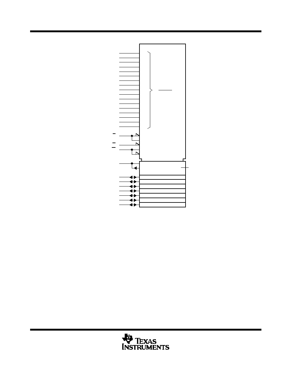
logic symbol
A
0
131 071
FLASH
MEMORY
131 072
◊
8
16
0
G1
[PWR DWN]
G2
1, 2 EN (READ)
1C3 (WRITE)
A, 3D
4
A0
A1
A2
A3
A4
A5
A6
A7
A8
A9
A10
A11
A12
A13
A14
A15
A16
E
G
W
DQ0
DQ1
DQ2
DQ3
DQ4
DQ5
DQ6
DQ7
12
11
10
9
8
7
6
5
27
26
23
25
4
28
29
3
2
22
24
31
13
14
15
17
18
19
20
21
A, Z4
This symbol is in accordance with ANSI / IEEE Std 91-1984 and IEC Publication 617-12.
Pin numbers shown are for the JDD package.
SMJ28F010B
131072 BY 8-BIT
FLASH MEMORY
SGMS738 ≠ APRIL 1998
4
POST OFFICE BOX 1443
∑
HOUSTON, TEXAS 77251≠1443
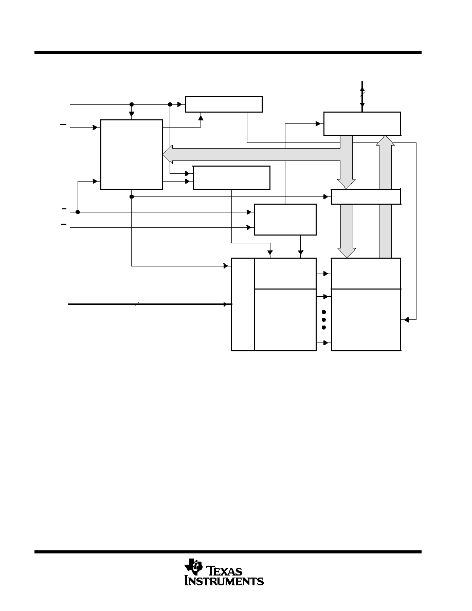
functional block diagram
Erase-Voltage Switch
VPP
A0 ≠ A16
A
d
d
r
e
s
s
L
a
t
c
h
Column Decoder
Row Decoder
Chip-Enable and
Output-Enable
Logic
DQ0 ≠ DQ7
Program-Voltage
Switch
W
1 048 576-Bit
Array Matrix
To Array
STB
STB
Input / Output Buffers
E
G
State Control
Program / Erase
Stop Timer
Command Register
Data Latch
Column Gating
8
17

SMJ28F010B
131072 BY 8-BIT
FLASH MEMORY
SGMS738 ≠ APRIL 1998
5
POST OFFICE BOX 1443
∑
HOUSTON, TEXAS 77251≠1443
operation
Table 1 lists the modes of operation for the device.
Table 1. Operation Modes
FUNCTION
MODE
VPP
(1)
E
(22)
G
(24)
A0
(12)
A9
(26)
W
(31)
DQ0 ≠ DQ7
(13 ≠ 15, 17 ≠ 21)
Read
VPPL
VIL
VIL
X
X
VIH
Data Out
Output Disable
VPPL
VIL
VIH
X
X
VIH
Hi-Z
Read
Standby and Write Inhibit
VPPL
VIH
X
X
X
X
Hi-Z
Read
Algorithm-Selection Mode
VPPL
VIL
VIL
VIL
VID
VIH
Manufacturer-Equivalent
Code 89h
g
PPL
IL
IL
VIH
ID
IH
Device-Equivalent Code B4h
Read
VPPH
VIL
VIL
X
X
VIH
Data Out
Read /
Output Disable
VPPH
VIL
VIH
X
X
VIH
Hi-Z
Write
Standby and Write Inhibit
VPPH
VIH
X
X
X
X
Hi-Z
Write
VPPH
VIL
VIH
X
X
VIL
Data In
X can be VIL or VIH.
VPPL
VCC + 2 V; VPPH is the programming voltage specified for the device. For more details, see the recommended operating conditions.
read / output disable
When the outputs of two or more SMJ28F010B devices are connected in parallel on the same bus, the output
of any particular device in the circuit can be read with no interference from the competing outputs of other
devices. Reading the output of the SMJ28F010B is enabled when a low-level signal is applied to the E and G
pins. All other devices in the circuit must have their outputs disabled by applying a high-level signal to one of
these pins.
standby and write inhibit
Active I
CC
current can be reduced from 30 mA to 1 mA by applying a high TTL level on E or to 100
µ
A with a
high CMOS level on E. In this mode, all outputs are in the high-impedance state. The SMJ28F010B draws active
current when it is deselected during programming, erasure, or program / erase verification. It continues to draw
active current until the operation is terminated.
algorithm-selection mode
The algorithm-selection mode provides access to a binary code identifying the correct programming and erase
algorithms. This mode is activated when A9 ( pin 26) is forced to V
ID
. Two identifier bytes are accessed by
toggling A0. All other addresses must be held low.
A0 low selects the manufacturer-equivalent code 89h, and
A0 high selects the device-equivalent code B4h, as shown in Table 2.
Table 2. Algorithm-Selection Modes
IDENTIFIERß
PINS
IDENTIFIERß
A0
DQ7
DQ6
DQ5
DQ4
DQ3
DQ2
DQ1
DQ0
HEX
Manufacturer-Equivalent Code
VIL
1
0
0
0
1
0
0
1
89
Device-Equivalent Code
VIH
1
0
1
1
0
1
0
0
B4
ß E =VIL, G = VIL, A1≠A8 = VIL, A9 = VID, A10≠A16 = VIL, VPP = VPPL.