
@vic
AV
1086
LINEAR INTEGRATED CIRCUIT
QW-R102-008,D
1.5A ADJUSTABLE/FIXED LOW
DROPOUT LINEAR REGULATOR
DESCRIPTION
The
@vic
AV
1086 and
AV
1086-1.8V,2.5V, 2.85V, 3.3V
and 5V are low dropout three-terminal regulators with 1.5A
output current capability. These devices have been
optimized for low voltage where transient response and
minimum input voltage are critical. The 2.85V version is
designed specifically to be used in Active Terminators for
SCSI bus.
Current limit is trimmed to ensure specified output
current and controlled short-circuit current. On-chip thermal
limiting provides protection against any combination of
overload and ambient temperatures that would create
excessive junction temperatures.
Unlike PNP type regulators where up to 10% of the
output current is wasted as quiescent current, the
quiescent current of the UZ1086 flows into the load,
increasing efficiency.
FEATURES
*Low dropout voltage
*Load regulation: 0.05% typical
*Trimmed current limit
*On-chip thermal limiting
*Three-terminal adjustable or fixed 1.8V, 2.5V, 2.85V,
3.3V, 5V
APPLICATIONS
*Active SCSI terminators
*High efficiency linear regulators
*Post regulators for switching supplies
*Battery charges
*5V to 3.3V linear regulators
*Motherboard clock supplies
TO-263
1
TO-252
1
SOT-223
TO-220
1
TO-263-3
1
1
1: ADJ/GND 2: V
OUT
3: V
IN
QW-R102-008,D
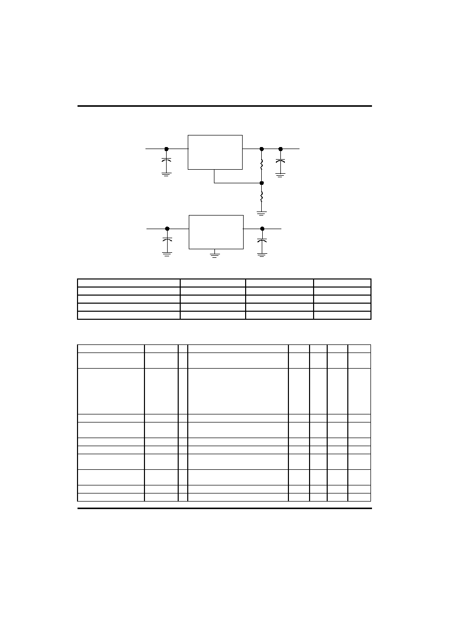
TYPICAL APPLICATIONS
R1
124
+
10
�F
+
22
�F
R2
24.9
1.5V at 1.5A
V
IN
=3.3V
V
IN
V
OUT
ADJ
V
OUT
=V
REF
(1+R2/R1)+I
Adj
*R2
+
10
�F
+
22
�F
2.85V at 1.5A
V
IN
=5V
V
IN
V
OUT
GND
AV
1086-2.85
AV
1086
ABSOLUTE MAXIMUM RATINGS
(Ta=25
�C, unless otherwise specified)
PARAMETER MIN
MAX
UNIT
V
IN
7.5
V
Operating Junction Temperature Range
0
125
�C
Storage Temperature Range
-65
150
�C
Lead Temperature (Soldering,10 sec)
300
�C
ELECTRICAL CHARACTERISTICS
(V
IN
7V, T
J
=25
�C, unless otherwise specified.
The*denotes specifications which apply over the specified operating temperature range.)
PARAMETER SYMBOL
TEST
CONDITIONS
MIN
TYP
MAX
UNIT
Reference Voltage
(note 3)
V
REF
*
1.5V(V
IN �
V
OUT
) 5.75V
10mAI
OUT
1A
1.225
1.25 1.275 V
Output Voltage
*
*
*
*
10mAI
OUT
1A
UZ1086-1.8V 3.3VV
IN
7V
UZ1086-2.5 4VV
IN
7V
UZ1086-2.85 4.35VV
IN
7V
UZ1086-3.3 4.8VV
IN
7V
UZ1086-5.0 6.5VV
IN
7V
1.764
2.450
2.793
3.234
4.900
1.80
2.50
2.85
3.30
5.00
1.836
2.550
2.907
3.366
5.100
V
V
V
V
Line Regulation (note1,2)
*
(V
OUT+
1.5V)V
IN
7V, I
OUT
=10mA
0.005
0.2 %
Load Regulation
(note1,2)
*
V
IN �
V
OUT
=2V, 10mAI
OUT
1A
0.05
0.5
%
Dropout Voltage
*
V
REF
=1%,I
OUT
=1.5A
1.3
1.5
V
Current Limit
*
V
IN �
V
OUT
=2V
1.6
2
A
Adjust Pin Current
(note 3)
IAdj *
35
120
�A
Adjust Pin Current
Change (note3)
* 1.5V(V
IN �
V
OUT
) 5.75V,
10mAI
OUT
1A
0.2 5
�A
Minimum Load Current
*
1.5V(V
IN �
V
OUT
) 5.75V 10
mA
Quiescent Current
*
V
IN
=V
OUT+
1.25V
4
13
mA
@vic
AV
1086
LINEAR INTEGRATED CIRCUIT

QW-R102-008,D
PARAMETER SYMBOL
TEST
CONDITIONS
MIN
TYP
MAX
UNIT
Ripple Rejection
f=120Hz,C
OUT
=22
�F, Tantalum
V
IN �
V
OUT
=3V, I
OUT
=1.5A
60 72 dB
Thermal Regulation
T
A
=25
�C,30ms pulse
0.004 0.02
%/W
Temperature Stability
*
0.5
%
Long-Term Stability
T
A
=125
�C, 1000hrs
0.03
1
%
RMS Output Noise
V
OUT
T
A
=25
�C, 10Hzf10kHz
0.003
%
Thermal Resistance
Junction to Case (note 4)
SOT-223
TO-252,TO-263,TO-220
15
3
�C/W
Thermal Shutdown
Junction Temperature
155
�C
Thermal Shutdown
Hysteresis
10
�C
Note:
1.
See thermal regulation specifications for changes in output voltage due to heating effects. Load and line
regulation are measured at a constant junction temperature by low duty cycle pulse testing.
2.
Line and load regulation are guaranteed up to the maximum power dissipation. Power dissipation is determined
by input/output differential and the output current. Guaranteed maximum output power will not be available over
the full input/output voltage range.
3.
AV
1086 adjustable only.
4.
With package soldered to 0.5 square inch copper area over backside ground plane or internal power plane,
Thermal Resistance Junction to Ambient can vary from 30
�C/W to more than 50�C/W. Other mounting
techniques may provide better thermal resistance than 30
�C/W.
@vic
AV
1086
LINEAR INTEGRATED CIRCUIT
QW-R102-008,D
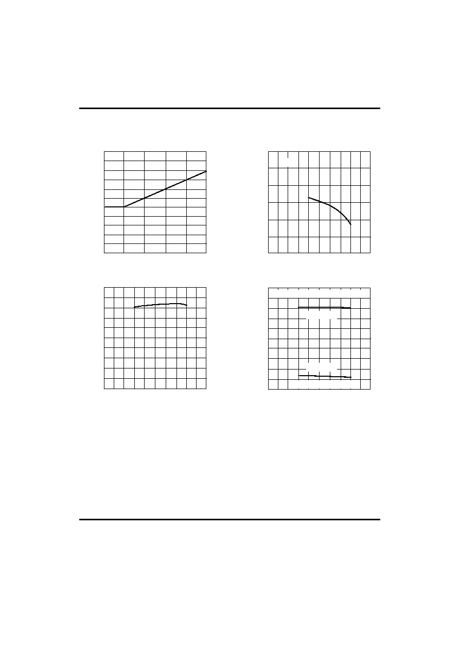
TYPICAL PERFORMANCE CHARACTERISTICS
0
0.3
0.6
0.9
1.2
0
0.5
0.6
0.7
0.8
0.9
Figure 1.Dropout Voltage vs.Output Current
Dr
op
ou
t
V
ol
t
ag
e (V
)
Output Current (A)
1.5
1.0
1.1
1.2
1.3
1.4
1.5
-75
-25
25
75
125
-50
-0.1
0
-0.05
50
Figure 2. Load Regulation vs.Temperature
D
r
o
pou
t
Volt
a
ge
Dev
i
at
ion
(
%)
Junction Temperature(� C)
175
0
100
0.0
5
150
0.1
-
0.15
-0.2
I=1A
-75
-25
25
75
125
-50
1.2
2
0
1.225
50
Figure 3.Reference Votage vs.Temperature
Re
f
er
en
c
e Volt
a
ge(
V)
Junction Temperature(� C)
175
1.23
100
1.23
5
150
1.25
1.21
1.2
1.205
1.215
1.24
5
1.24
-75
-25
25
75
125
-50
3.4
0
3.45
50
Figure 4.Output Voltage vs.Temperature
R
e
f
e
re
nc
e V
o
l
tage
(
V
)
Junction Temperature(� C)
175
3.5
100
3.55
150
3.7
3.3
3.2
3.25
3.35
3.65
3.6
V
OUT
SET WITH 1% RESISTORS
V
OUT
=3.6V
V
OUT
=3.3V
UZ1086 adjustable Only
@vic
AV
1086
LINEAR INTEGRATED CIRCUIT
QW-R102-008,D
-75
-25
25
75
125
-50
0
1.5
50
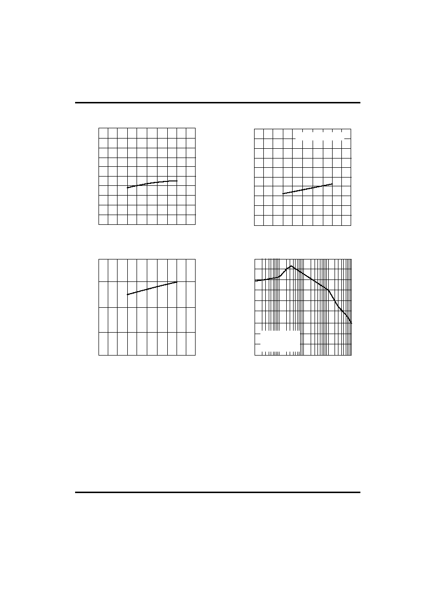
Figure 7. Short-Circuit Current vs.Temperature
S
h
o
r
t-
C
i
r
c
u
i
t C
u
r
r
e
n
t
(
A
)
Junction Temperature(� C)
175
100
1.7
5
150
2.0
1.25
1.0
-75
-25
25
75
125
-50
2
0
50
Figure 5.Minimum Load Current vs.Temperature
Mi
n
i
mum Lo
ad
Cur
r
en
t
(
mA)
Junction Temperature(� C)
175
3
100
150
5
1
0
4
-75
-25
25
75
125
-50
40
0
50
50
Figure 6.Adjust Pin Current vs.Temperature
Adjust
Pin C
u
r
r
e
n
t
(
�
A)
Junction Temperature(� C)
175
60
100
70
150
100
20
0
10
30
90
80
Note1.UZ1086 Only
0
90
Frequency (Hz)
Figure 8. Ripple Rejection vs.Frequency
R
i
p
p
l
e
R
e
j
e
c
t
i
on
(
d
B
)
100
1K
10K
100K
V
IN
-V
OUT
=3V
0.5<V
RIPPLE
<2V
I
OUT
=1A
10
10
20
30
40
50
60
70
80
@vic
AV
1086
LINEAR INTEGRATED CIRCUIT