 | –≠–ª–µ–∫—Ç—Ä–æ–Ω–Ω—ã–π –∫–æ–º–ø–æ–Ω–µ–Ω—Ç: AZ100E111 | –°–∫–∞—á–∞—Ç—å:  PDF PDF  ZIP ZIP |
AZ10E111
AZ100E111
ECL/PECL 1:9 Differential Clock Driver
1630 S. STAPLEY DR., SUITE 125
∑
MESA, ARIZONA 85204
∑
USA
∑
(480) 962-5881
∑
FAX (480) 890-2541
www.azmicrotek.com
ARIZONA MICROTEK, INC.
FEATURES
∑
Low Skew
∑
Differential Design
∑
Clock Enable
∑
V
BB
Output
∑
Operating Range of 4.2V to 5.46V
∑
75k
Internal Input Pulldown Resistors
∑
Direct Replacement for ON Semiconductor
MC10E111 & MC100E111
DESCRIPTION
The AZ10/100E111 is a low skew 1-to-9 differential driver, designed with clock distribution in mind. The IN
signal is fanned-out to nine identical differential outputs. An Enable input is also provided. A HIGH disables the
device by forcing all Q outputs LOW and all Q
Ø outputs HIGH.
The AZ100E111 provides a V
BB
output for single-ended use or a DC bias reference for AC coupling to the
device. For single≠ended input applications, the V
BB
reference should be connected to one side of the IN/IN
ØØ
differential input pair. The input signal is then fed to the other IN/IN
ØØ input. The V
BB
pin should be used only as a
bias for the E111 as its sink/source capability is limited. When used, the V
BB
pin should be bypassed to ground via a
0.01
µ
F capacitor.
The device is specifically designed, modeled and produced with low skew as the key goal. Optimal design and
layout serve to minimize gate-to-gate skew within-device, and empirical modeling is used to determine process
control limits that ensure consistent t
pd
distributions from lot-to-lot. The net result is a dependable, low skew device.
To ensure that the tight skew specification is met, both sides of the differential output must be terminated into
50
, even if only one side is used. In most applications all nine differential pairs will be used and therefore
terminated. In the case where fewer than nine pairs are used, it is necessary to terminate at least the output pairs on
the same package side (i.e. sharing the same V
CCO
) as the pair(s) being used on that side, in order to maintain
minimum skew. Failure to do this will result in small degradations of propagation delay (on the order of 10-20ps) of
the output(s) being used that, while not being catastrophic to most designs, will mean a loss of skew margin.
NOTE: Specifications in the ECL/PECL tables are valid when thermal equilibrium is established.
PACKAGE AVAILABILITY
PACKAGE PART
NO. MARKING
PLCC 28
AZ10E111FN
AZM10E111
PLCC 28 T&R AZ10E111FNR2
AZM10E111
PLCC 28
AZ100E111FN
AZM100E111
PLCC 28 T&R AZ100E111FNR2 AZM100E111
AZ10E111
AZ100E111
October 2001 * REV - 2
www.azmicrotek.com
2
Absolute Maximum Ratings are those values beyond which device life may be impaired.
Symbol Characteristic
Rating
Unit
V
CC
PECL Power Supply (V
EE
= 0V)
0 to +8.0
Vdc
V
I
PECL Input Voltage (V
EE
= 0V)
0 to +6.0
Vdc
V
EE
ECL Power Supply (V
CC
= 0V)
-8.0 to 0
Vdc
V
I
ECL Input Voltage (V
CC
= 0V)
-6.0 to 0
Vdc
I
OUT
Output Current
--- Continuous
--- Surge
50
100
mA
T
A
Operating Temperature Range
-40 to +85
∞
C
T
STG
Storage Temperature Range
-65 to +150
∞
C
10K ECL DC Characteristics (V
EE
= -4.94V to -5.46V, V
CC
= V
CCO
= GND)
-40
∞
C
0
∞
C
25
∞
C
85
∞
C
Symbol
Characteristic
Min Typ Max Min Typ Max Min Typ Max Min Typ Max
Unit
V
OH
Output
HIGH
Voltage
1
-1080
-890
-1020 -840
-980 -810
-910 -720 mV
V
OL
Output LOW Voltage
1
-1950 -1650
-1950 -1630
-1950 -1630
-1950 -1595 mV
V
IH
Input
HIGH
Voltage -1230 -890
-1170 -840
-1130 -810
-1060 -720 mV
V
IL
Input
LOW
Voltage -1950 -1500
-1950 -1480
-1950 -1480
-1950 -1445 mV
V
BB
Reference
Voltage
-1430 -1300
-1380 -1270
-1350 -1250
-1310 -1190 mV
I
IH
Input
HIGH
Current
150
150
150
150
µ
A
I
IL
Input
LOW
Current 0.5 0.5 0.5 0.5
µ
A
I
EE
Power
Supply
Current 48 60 48 60 48 60 48 60 mA
1.
Each output is terminated through a 50
resistor to V
CC
≠ 2V.
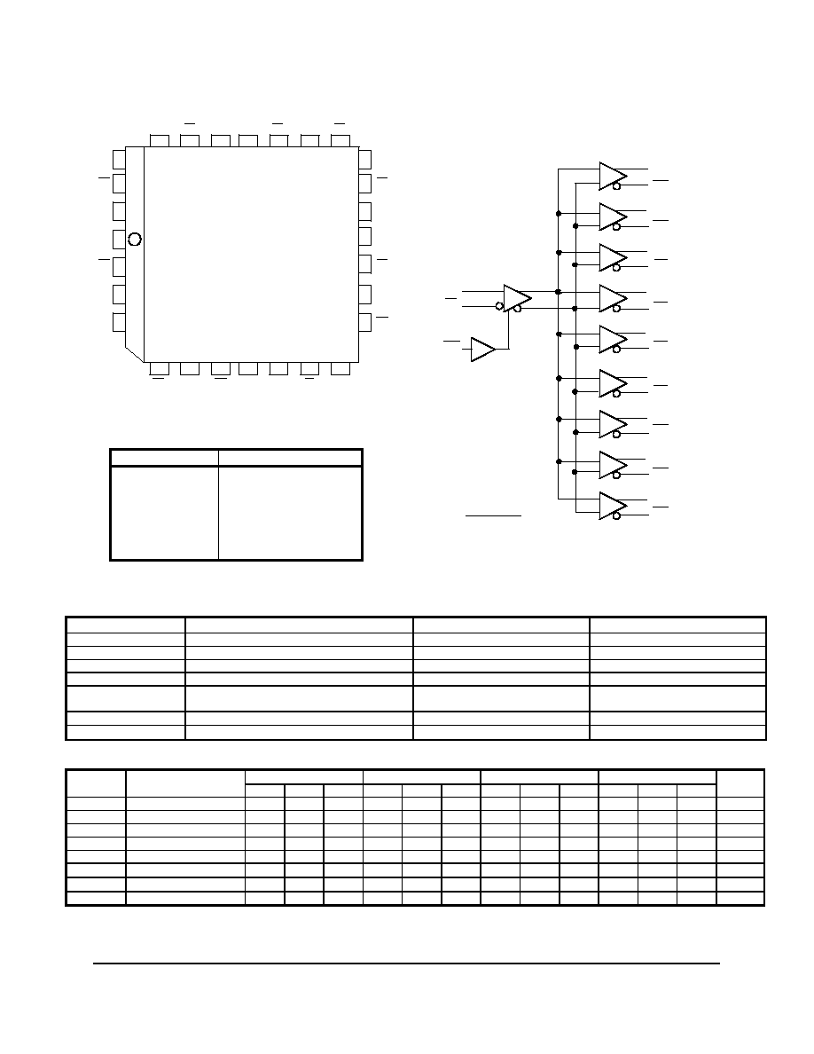
LOGIC SYMBOL
V BB
IN
IN
EN
Q0
Q0
Q1
Q1
Q2
Q2
Q3
Q3
Q4
Q4
Q5
Q5
Q6
Q6
Q7
Q7
Q8
Q8
26
27
28
1
2
3
4
Q0
Q0
Q1
Q2
V
CCO
Q1
Q2
Q3
Q3
V
CC
Q5
V
CCO
Q5
Q6
Q6
Q7
V
CCO
Q8
Q8
V
EE
IN
NC
25
24
23
22
21
20
19
18
17
16
15
14
13
12
11
10
9
8
7
6
5
V
BB
IN
EN
Q4
Q4
Q7
Pinout: 28-Lead PLCC
(Top View)
PIN DESCRIPTION
PIN FUNCTION
IN, IN
ØØ Differential
Input
Pair
EN
ØØ Enable
Q0, Q0
ØØ - Q8, Q8
ØØ Differential
Outputs
V
BB
V
BB
Output
V
CC
, V
CCO
Positive Supply
V
EE
Negative Supply
AZ10E111
AZ100E111
October 2001 * REV - 2
www.azmicrotek.com
3
10K PECL DC Characteristics (V
EE
= GND, V
CC
= V
CCO
= +5.0V)
-40
∞
C 0
∞
C 25
∞
C 85
∞
C
Symbol Characteristic
Min Typ Max
Min
Typ
Max
Min
Typ
Max Min Typ
Max
Unit
V
OH
Output
HIGH
Voltage
1,2
3920 4110
3980 4160
4020 4190
4090 4280 mV
V
OL
Output LOW Voltage
1,2
3050 3350
3050 3370
3050 3370
3050 3405 mV
V
IH
Input
HIGH
Voltage
1
3770 4110
3830 4160
3870 4190
3940 4280 mV
V
IL
Input LOW Voltage
1
3050 3500
3050 3520
3050 3520
3050 3555 mV
V
BB
Reference
Voltage
1
3570 3700
3620 3730
3650 3750
3690 3810 mV
I
IH
Input
HIGH
Current
150 150 150 150
µ
A
I
IL
Input
LOW
Current
0.5 0.5 0.5 0.5
µ
A
I
EE
Power
Supply
Current 48 60 48 60 48 60 48 60 mA
1.
For supply voltages other that 5.0V, use the ECL table values and ADD supply voltage value.
2.
Each output is terminated through a 50
resistor to V
CC
≠ 2V.
100K ECL DC Characteristics (V
EE
= -4.2V to -5.46V, V
CC
= V
CCO
= GND)
-40
∞
C
0
∞
C
25
∞
C
85
∞
C
Symbol
Characteristic
Min Typ Max Min Typ Max Min Typ Max Min Typ Max
Unit
V
OH
Output
HIGH
Voltage
1
-1085 -1005 -880 -1025 -955 -880 -1025 -955 -880 -1025 -955 -880 mV
V
OL
Output LOW Voltage
1
-1830 -1695 -1555 -1810 -1705 -1620 -1810 -1705 -1620 -1810 -1705 -1620 mV
V
IH
Input
HIGH
Voltage -1165 -880
-1165 -880
-1165 -880
-1165 -880 mV
V
IL
Input
LOW
Voltage -1810 -1475
-1810 -1475
-1810 -1475
-1810 -1475 mV
V
BB
Reference
Voltage
-1380 -1260
-1380 -1260
-1380 -1260
-1380 -1260 mV
I
IH
Input
HIGH
Current
150
150
150
150
µ
A
I
IL
Input
LOW
Current 0.5 0.5 0.5 0.5
µ
A
I
EE
Power
Supply
Current 48 60 48 60 48 60 55 69 mA
1.
Each output is terminated through a 50
resistor to V
CC
≠ 2V.
100K PECL DC Characteristics (V
EE
= GND, V
CC
= V
CCO
= +5.0V)
-40
∞
C 0
∞
C 25
∞
C 85
∞
C
Symbol Characteristic
Min Typ Max
Min
Typ
Max
Min
Typ
Max Min Typ
Max
Unit
V
OH
Output
HIGH
Voltage
1,2
3915 3995 4120 3975 4045 4120 3975 4045 4120 3975 4045 4120 mV
V
OL
Output LOW Voltage
1,2
3170 3305 3445 3190 3295 3380 3190 3295 3380 3190 3295 3380 mV
V
IH
Input
HIGH
Voltage
1
3835 4120
3835 4120
3835 4120
3835 4120 mV
V
IL
Input LOW Voltage
1
3190 3525
3190 3525
3190 3525
3190 3525 mV
V
BB
Reference
Voltage
1
3620 3740
3620 3740
3620 3740
3620 3740 mV
I
IH
Input
HIGH
Current
150 150 150 150
µ
A
I
IL
Input
LOW
Current
0.5 0.5 0.5 0.5
µ
A
I
EE
Power
Supply
Current 48 60 48 60 48 60 55 69 mA
1.
For supply voltages other that 5.0V, use the ECL table values and ADD supply voltage value.
2.
Each output is terminated through a 50
resistor to V
CC
≠ 2V.

AZ10E111
AZ100E111
October 2001 * REV - 2
www.azmicrotek.com
4
AC Characteristics (V
EE
=10E(-4.94V to -5.46V), 100E(-4.2V to -5.46V); V
CC
=V
CCO
=GND or V
EE
=GND;
V
CC
=V
CCO
= 10E(+4.94V to +5.46V), 100E(+4.2V to +5.46V) )
-40
∞
C
0
∞
C
25
∞
C
85
∞
C
Symbol
Characteristic
Min Typ Max Min Typ Max Min Typ Max Min Typ Max
Unit
t
PLH
/ t
PHL
Propagation Delay
to Output IN (Diff)
1
IN (SE)
2
Enable
3
Disable
3
380
280
400
400
680
780
900
900
460
410
450
450
560
610
850
850
480
430
450
450
580
630
850
850
510
460
450
450
610
660
850
850
ps
t
S
Setup Time EN
ØØ to IN
5
250
0 200
0 200
0 200
0 ps
t
H
Hold Time IN to EN
ØØ
6
50 -200 0 -200 0 -200 0 -200 ps
t
R
Release Time EN
ØØ to IN
7
350
100 300
100 300
100 300
100 ps
t
SKEW
Within-Device
Skew
4
25 75 25 50 25 50 25 50
ps
V
PP
(AC) Minimum
Input
Swing
8
250 250 250 250 mV
V
CMR
Common Mode Range
9
V
CC
-
1.6
V
CC
-
0.4
V
CC
-
1.6
V
CC
-
0.4
V
CC
-
1.6
V
CC
-
0.4
V
CC
-
1.6
V
CC
-
0.4
V
t
r
/ t
f
Rise/Fall
Time
250 650
275 600
275 600
275 600
ps
1. The differential propagation delay is defined as the delay from the crossing points of the differential input signals to the crossing point of the
differential output signals.
2. The single-ended propagation delay is defined as the delay from the 50% point of the input signal to the 50% point of the output signal.
3. Enable is defined as the propagation delay from the 50% point of a negative transition on EN
ØØ to the 50% point of a positive transition on Q (or a
negative transition on Q
Ø). Disable is defined as the propagation delay from the 50% point of a positive transition on EN
ØØ to the 50% point of a
negative transition on Q (or a positive transition on Q
Ø).
4. The within-device skew is defined as the worst-case difference between any two similar delay paths within a single device.
5. The setup time is the minimum time that EN
ØØ must be asserted prior to the next transition of IN/ IN
ØØ to prevent an output response greater than
±
75mV to that IN/ IN
ØØ transition (see Figure 1).
6. The hold time is the minimum time that EN
ØØ must remain asserted after a negative going IN or a positive going IN
ØØ to prevent an output response
greater than
±
75 mV to that IN/ IN
ØØ transition (see Figure 2).
7. The release time is the minimum time that EN
ØØ must be de-asserted prior to the next IN/ IN
ØØ transition to ensure an output response that meets the
specified IN to Q propagation delay and output transition times (see Figure 3).
8. V
PP
(min) is defined as the minimum peak-to-peak input differential voltage which will cause no increase in the propagation delay. The V
PP
(min)
is AC limited for the E111, because differential input as low as 50 mV will still produce full ECL levels at the output.
9. V
CMR
is defined as the range within which the V
IH
level may vary, with the device still meeting the propagation delay specification. The V
IL
level
must be such that the peak-to-peak voltage is less than 1.0V and greater than or equal to V
PP
(min).
IN
IN
EN
H
IN
IN
EN
IN
IN
EN

AZ10E111
AZ100E111
October 2001 * REV - 2
www.azmicrotek.com
5
PACKAGE DIAGRAM
PLCC 28
MILLIMETERS INCHES
DIM
MIN MAX MIN MAX
A
12.32 12.57 0.485 0.495
B
12.32 12.57 0.485 0.495
C
4.20 4.57 0.165 0.180
E
2.29 2.79 0.090 0.110
F
0.33 0.48 0.013 0.019
G
1.27 BSC
0.050 BSC
H
0.66 0.81 0.026 0.032
J
0.51 0.020
K
0.64 0.025
R
11.43 11.58 0.450 0.456
U
11.43 11.58 0.450 0.456
V
1.07 1.21 0.042 0.048
W
1.07 1.21 0.042 0.048
X
1.07 1.42 0.042 0.056
T
0.50 0.020
Z
2
O
10
O
2
O
10
O
G1
10.42 10.92 0.410 0.430
K1
1.02 0.040
NOTES:
1.
DATUMS ≠L-, -M-, AND ≠N- DETERMINED
WHERE TOP OF LEAD SHOULDER EXITS
PLASTIC BODY AT MOLD PARTING LINE.
2.
DIMENSION G1, TRUE POSITION TO BE
MEASURED AT DATUM ≠T-, SEATING PLANE.
3.
DIMENSIONS R AND U DO NOT INCLUDE
MOLD FLASH. ALOWABLE MOLD FLASH IS
0.010mm (0.250in.) PER SIDE.
4.
DIMENSIONING AND TOLERANCING PER ANSI
Y14.5M, 1982.
5.
CONTROLLING DIMENSION: INCH.
6.
THE PACKAGE TOP MAY BE SMALLER THAN
THE PACKGE BOTTOM BY UP TO 0.012mm
(0.300in.). DIMENSIONS R AND U ARE
DETERMINED AT THE OUTERMOST
EXTREMES OF THE PLASTIC BODY
EXCLUSIVE OF MOLD FLASH, THE BAR
BURRS, GATE BURRS AND INTERLEAD FLASH,
BUT INCLUDING ANY MISMATCH BETWEEN
THE TOP AND BOTTOM OF THE PLASTIC
BODY.
7.
DIMENSION H DOES NOT INCLUDE DAMBAR
PROTRUSION OR INTRUSION. THE DAMBAR
PROTRUSION(S) SHALL NOT CAUSE THE H
DIMENSION TO BE SMALLER THAN 0.025mm
(0.635in.).