
AZ10EL16
AZ100EL16
ECL/PECL Differential Receiver
1630 S. STAPLEY DR., SUITE 125
∑
MESA, ARIZONA 85204
∑
USA
∑
(480) 962-5881
∑
FAX (480) 890-2541
www.azmicrotek.com
ARIZONA MICROTEK, INC.
FEATURES
∑
250ps Propagation Delay
∑
High Bandwidth Output Transitions
∑
75k
Internal Input Pulldown Resistors
∑
Direct Replacement for ON Semiconductor
MC10EL16 & MC100EL16
DESCRIPTION
The AZ10/100EL16 is a differential receiver. The device is functionally equivalent to the E116 device with
higher performance capabilities. With output transition times significantly faster than the E116, the EL16 is ideally
suited for interfacing with high frequency sources.
The EL16 provides a V
BB
output for either single-ended use or a DC bias reference for AC coupling to the
device. For single-ended input applications, the V
BB
reference should be connected to one side of the D/D
Ø differential
input pair. The input signal is then fed to the other D/D
Ø input. The V
BB
pin can support 1.0mA sink/source current.
When used, the V
BB
pin should be bypassed to ground via a 0.01
µ
F capacitor.
Under open input conditions (pulled to V
EE
) internal input clamps will force the Q output LOW.
NOTE: Specifications in the ECL/PECL tables are valid when thermal equilibrium is established.
LOGIC DIAGRAM AND PINOUT ASSIGNMENT
8
5
6
7
4
3
2
1
VCC
D
VEE
NC
Q
Q
VBB
D
PACKAGE AVAILABILITY
PACKAGE PART
NO. MARKING
SOIC 8
AZ10EL16D
AZM10EL16
SOIC 8 T&R
AZ10EL16DR1
AZM10EL16
SOIC 8 T&R
AZ10EL16DR2
AZM10EL16
SOIC 8
AZ100EL16D
AZM100EL16
SOIC 8 T&R
AZ100EL16DR1 AZM100EL16
SOIC 8 T&R
AZ100EL16DR2 AZM100EL16
TSSOP 8
AZ10EL16T
AZTEL16
TSSOP 8 T&R AZ10EL16TR1
AZTEL16
TSSOP 8 T&R AZ10EL16TR2
AZTEL16
TSSOP 8
AZ100EL16T
AZHEL16
TSSOP 8 T&R AZ100EL16TR1 AZHEL16
TSSOP 8 T&R AZ100EL16TR2 AZHEL16
PIN DESCRIPTION
PIN FUNCTION
D, D
Ø Data
Inputs
Q, Q
Ø Data
Outputs
V
BB
Reference Voltage Output
V
CC
Positive Supply
V
EE
Negative Supply
NC No
Connect

AZ10EL16
AZ100EL16
October 2001 * REV - 2
www.azmicrotek.com
2
Absolute Maximum Ratings are those values beyond which device life may be impaired.
Symbol Characteristic
Rating
Unit
V
CC
PECL Power Supply (V
EE
= 0V)
0 to +8.0
Vdc
V
I
PECL Input Voltage (V
EE
= 0V)
0 to +6.0
Vdc
V
EE
ECL Power Supply (V
CC
= 0V)
-8.0 to 0
Vdc
V
I
ECL Input Voltage (V
CC
= 0V)
-6.0 to 0
Vdc
I
OUT
Output Current
--- Continuous
--- Surge
50
100
mA
T
A
Operating Temperature Range
-40 to +85
∞
C
T
STG
Storage Temperature Range
-65 to +150
∞
C
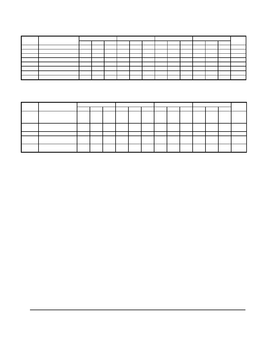
10K ECL DC Characteristics (V
EE
= -4.75V to -5.5V, V
CC
= GND)
-40
∞
C
0
∞
C
25
∞
C
85
∞
C
Symbol
Characteristic
Min Typ Max Min Typ Max Min Typ Max Min Typ Max
Unit
V
OH
Output
HIGH
Voltage
1
-1080
-890
-1020 -840
-980 -810
-910 -720 mV
V
OL
Output LOW Voltage
1
-1950 -1650
-1950 -1630
-1950 -1630
-1950 -1595 mV
V
IH
Input
HIGH
Voltage -1230 -890
-1170 -840
-1130 -810
-1060 -720 mV
V
IL
Input
LOW
Voltage -1950 -1500
-1950 -1480
-1950 -1480
-1950 -1445 mV
V
BB
Reference
Voltage
-1430 -1300
-1380 -1270
-1350 -1250
-1310 -1190 mV
I
IH
Input
HIGH
Current
150
150
150
150
µ
A
I
IL
Input
LOW
Current 0.5 0.5 0.5 0.5
µ
A
I
EE
Power
Supply
Current 18 22 18 22 18 22 18 22 mA
1.
Each output is terminated through a 50
resistor to V
CC
≠ 2V.
10K PECL DC Characteristics (V
EE
= GND, V
CC
= +5.0V)
-40
∞
C 0
∞
C 25
∞
C 85
∞
C
Symbol Characteristic
Min Typ Max
Min
Typ
Max
Min
Typ
Max Min Typ
Max
Unit
V
OH
Output
HIGH
Voltage
1,2
3920 4110
3980 4160
4020 4190
4090 4280 mV
V
OL
Output LOW Voltage
1,2
3050 3350
3050 3370
3050 3370
3050 3405 mV
V
IH
Input
HIGH
Voltage
1
3770 4110
3830 4160
3870 4190
3940 4280 mV
V
IL
Input LOW Voltage
1
3050 3500
3050 3520
3050 3520
3050 3555 mV
V
BB
Reference
Voltage
1
3570 3700
3620 3730
3650 3750
3690 3810 mV
I
IH
Input
HIGH
Current
150 150 150 150
µ
A
I
IL
Input
LOW
Current
0.5 0.5 0.5 0.5
µ
A
I
EE
Power
Supply
Current 18 22 18 22 18 22 18 22 mA
1.
For supply voltages other that 5.0V, use the ECL table values and ADD supply voltage value.
2.
Each output is terminated through a 50
resistor to V
CC
≠ 2V.
100K ECL DC Characteristics (V
EE
= -4.2V to -5.5V, V
CC
= GND)
-40
∞
C
0
∞
C
25
∞
C
85
∞
C
Symbol Characteristic
Min Typ Max Min Typ Max Min Typ Max Min Typ Max
Unit
V
OH
Output
HIGH
Voltage
1
-1085 -1005 -880 -1025 -955 -880 -1025 -955 -880 -1025 -955 -880 mV
V
OL
Output LOW Voltage
1
-1830 -1695 -1555 -1810 -1705 -1620 -1810 -1705 -1620 -1810 -1705 -1620 mV
V
IH
Input
HIGH
Voltage -1165 -880
-1165 -880
-1165 -880
-1165 -880 mV
V
IL
Input
LOW
Voltage -1810 -1475
-1810 -1475
-1810 -1475
-1810 -1475 mV
V
BB
Reference
Voltage
-1380 -1260
-1380 -1260
-1380 -1260
-1380 -1260 mV
I
IH
Input
HIGH
Current
150
150
150
150
µ
A
I
IL
Input
LOW
Current 0.5 0.5 0.5 0.5
µ
A
I
EE
Power
Supply
Current 18 22 18 22 18 22 21 26 mA
1.
Each output is terminated through a 50
resistor to V
CC
≠ 2V.
AZ10EL16
AZ100EL16
October 2001 * REV - 2
www.azmicrotek.com
3
100K PECL DC Characteristics (V
EE
= GND, V
CC
= +5.0V)
-40
∞
C 0
∞
C 25
∞
C 85
∞
C
Symbol Characteristic
Min Typ Max
Min
Typ
Max
Min
Typ
Max Min Typ
Max
Unit
V
OH
Output
HIGH
Voltage
1,2
3915 3995 4120 3975 4045 4120 3975 4045 4120 3975 4045 4120 mV
V
OL
Output LOW Voltage
1,2
3170 3305 3445 3190 3295 3380 3190 3295 3380 3190 3295 3380 mV
V
IH
Input
HIGH
Voltage
1
3835 4120
3835 4120
3835 4120
3835 4120 mV
V
IL
Input LOW Voltage
1
3190 3525
3190 3525
3190 3525
3190 3525 mV
V
BB
Reference
Voltage
1
3620 3740
3620 3740
3620 3740
3620 3740 mV
I
IH
Input
HIGH
Current
150 150 150 150
µ
A
I
IL
Input
LOW
Current
0.5 0.5 0.5 0.5
µ
A
I
EE
Power
Supply
Current 18 22 18 22 18 22 21 26 mA
1.
For supply voltages other that 5.0V, use the ECL table values and ADD supply voltage value.
2.
Each output is terminated through a 50
resistor to V
CC
≠ 2V.
AC Characteristics (V
EE
=10E(-4.75V to -5.5V), 100E(-4.2V to -5.5V); V
CC
=GND or V
EE
=GND; V
CC
=10E(+4.75V to +5.5V),
100E(+4.2V to +5.5V) )
-40
∞
C
0
∞
C
25
∞
C
85
∞
C
Symbol
Characteristic
Min Typ Max Min Typ Max Min Typ Max Min Typ Max
Unit
t
PLH
/ t
PHL
Propagation Delay
to Output (Diff)
(SE)
125
75
250
250
375
425
175
125
250
250
325
375
175
125
250
250
325
375
205
155
280
280
355
405
ps
t
SKEW
Duty Cycle Skew
1
(Diff)
5 5 20 5 20 5 20 ps
V
PP
(AC) Minimum
Input
Swing
2
150 150 150 150 mV
V
CMR
Common Mode Range
3
V
CC
≠
2.0
V
CC
≠
0.4
V
CC
≠
2.0
V
CC
≠
0.4
V
CC
≠
2.0
V
CC
≠
0.4
V
CC
≠
2.0
V
CC
≠
0.4
V
t
r
/ t
f
Output Rise/Fall Times
Q (20% - 80%)
100 350
100 350
100 350
100 350 ps
1. Duty cycle skew is the difference between a t
PLH
and t
PHL
propagation delay through a device.
2. V
PP
is the minimum peak-to-peak differential input swing for which AC parameters are guaranteed. The device has a DC gain of
40.
3. The
V
CMR
range is referenced to the most positive side of the differential input signal. Normal operation is obtained if the HIGH level falls within the
specified range and the peak-to-peak voltage lies between V
PP
(min) and 1V.
AZ10EL16
AZ100EL16
October 2001 * REV - 2
www.azmicrotek.com
4
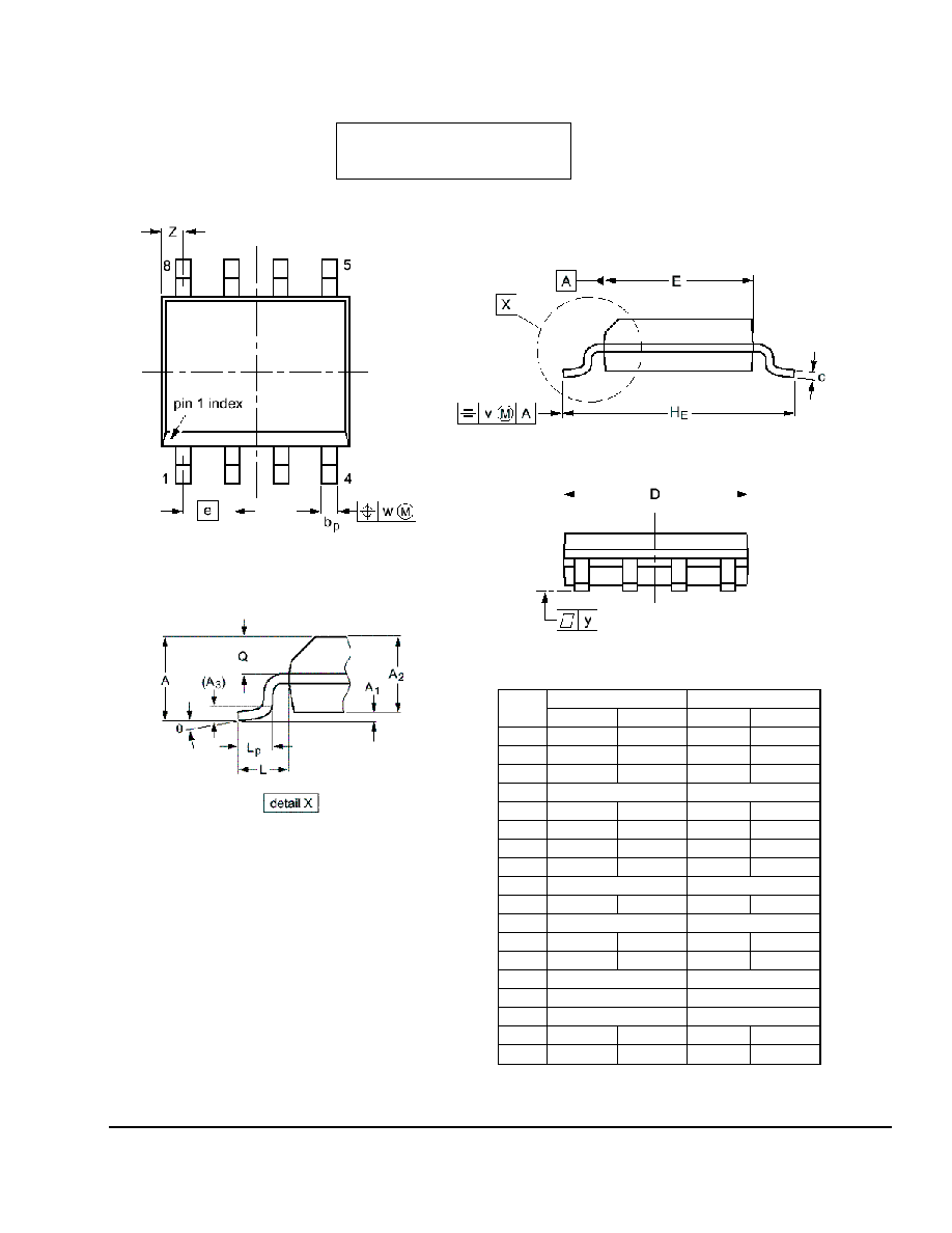
MILLIMETERS INCHES
DIM
MIN MAX MIN MAX
A
1.75 0.069
A
1
0.10 0.25 0.004
0.010
A
2
1.25 1.45 0.049
0.057
A
3
0.25 0.01
b
p
0.36 0.49 0.014
0.019
c
0.19 0.25
0.0075
0.0100
D
4.8 5.0 0.19
0.20
E
3.8 4.0 0.15
0.16
e
1.27 0.050
H
E
5.80 6.20 0.228
0.244
L
1.05 0.041
L
p
0.40 1.00 0.016
0.039
Q
0.60 0.70 0.024
0.028
v
0.25 0.01
w
0.25 0.01
y
0.10 0.004
Z
0.30 0.70 0.012
0.028
0
O
8
O
0
O
8
O
NOTES:
1.
DIMENSIONS D AND E DO NOT
INCLUDE MOLD PROTRUSION.
2. MAXIMUM
MOLD
PROTRUSION
FOR D IS 0.15mm.
3. MAXIMUM
MOLD
PROTRUSION
FOR E IS 0.25mm.
PACKAGE DIAGRAM
SOIC 8
AZ10EL16
AZ100EL16
October 2001 * REV - 2
www.azmicrotek.com
5
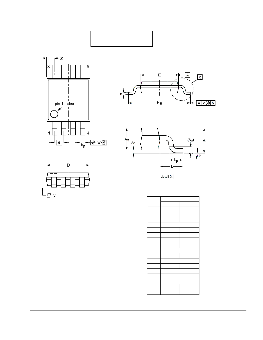
PACKAGE DIAGRAM
TSSOP 8
MILLIMETERS
DIM
MIN MAX
A
1.10
A
1
0.05 0.15
A
2
0.80 0.95
A
3
0.25
b
p
0.25 0.45
c
0.15 0.28
D
2.90 3.10
E
2.90 3.10
e
0.65
H
E
4.70 5.10
L
0.94
L
p
0.40 0.70
v
0.10
w
0.10
y
0.10
Z
0.35 0.70
0
O
6
O
NOTES:
1.
DIMENSIONS D AND E DO NOT
INCLUDE MOLD PROTRUSION.
2. MAXIMUM
MOLD
PROTRUSION
FOR D IS 0.15mm.
3. MAXIMUM
MOLD
PROTRUSION
FOR E IS 0.25mm.