AZ100ELT21
Differential PECL to CMOS/TTL Translator
1630 S. STAPLEY DR., SUITE 125
∑ MESA, ARIZONA 85204 ∑ USA ∑ (480) 962-5881 ∑ FAX (480) 890-2541
www.azmicrotek.com
ARIZONA MICROTEK, INC.
FEATURES
∑ 3.5ns Typical Propagation Delay
∑ Differential PECL Inputs
∑ CMOS/TTL Outputs
∑ Flow Through Pinouts
∑ Operating Range of 3.0V to 5.5V
∑ Direct Replacement for ON Semiconductor
MC100ELT21
∑ Use AZ100ELT21 for 10K Applications
DESCRIPTION
The AZ100ELT21 is a differential PECL to CMOS/TTL translator. Because PECL (Positive ECL) levels are
used, only V
CC
and ground are required. The small outline 8-lead packaging and the single gate of the ELT21 makes
it ideal for those applications where space, performance and low power are at a premium.
The ELT21 provides a V
BB
output for single-ended use or a DC bias reference for AC coupling to the device.
For single-ended input applications, the V
BB
reference should be connected to one side of the D0/D0
ØØ differential
input pair. The input signal is then fed to the other D0/D0
ØØ input. The V
BB
pin should be used only as a bias for the
ELT21 as its sink/source capability is limited. When used, the V
BB
pin should be bypassed to ground via a 0.01
µF
capacitor.
NOTE: Specification in ECL/PECL tables are valid when thermal equilibrium is established.
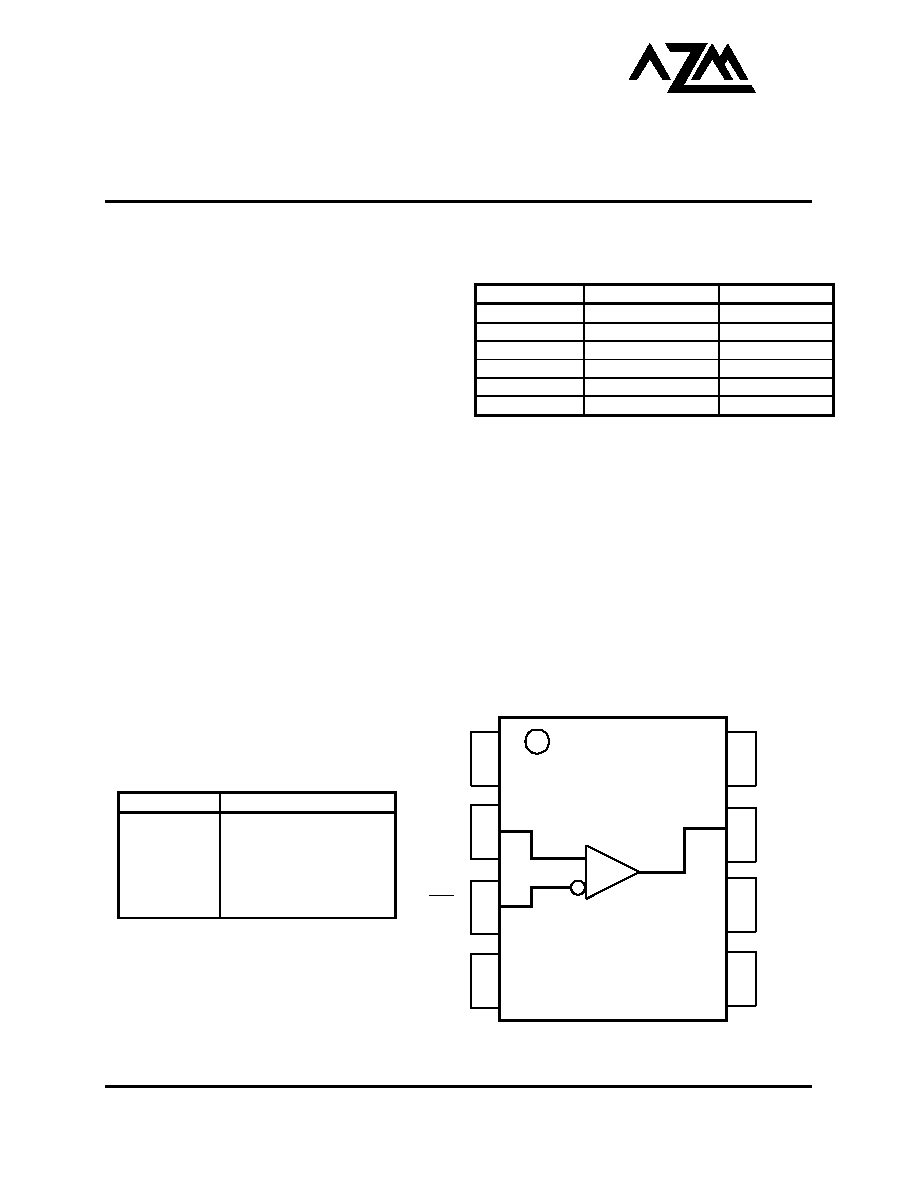
LOGIC DIAGRAM AND PINOUT ASSIGNMENT
PACKAGE AVAILABILITY
PACKAGE PART
NO. MARKING
SOIC 8
AZ100ELT21D
AZM100ELT21
SOIC 8 T&R
AZ100ELT21DR1
AZM100ELT21
SOIC 8 T&R
AZ100ELT21DR2
AZM100ELT21
TSSOP 8
AZ100ELT21T
AZHLT21
TSSOP 8 T&R AZ100ELT21TR1
AZHLT21
TSSOP 8 T&R AZ100ELT21TR2
AZHLT21
PIN DESCRIPTION
PIN FUNCTION
Q CMOS/TTL
Output
D0, D0
ØØ Differential
Inputs
V
CC
Positive
Supply
V
BB
Reference Voltage Output
GND Ground
NC No
Connect
8
5
6
7
4
3
2
1
VCC
Q
GND
NC
D0
VBB
D0
NC
PECL
CMOS/TTL

AZ100ELT21
March 2002 * REV - 3
www.azmicrotek.com
2
Absolute Maximum Ratings are those values beyond which device life may be impaired.
Symbol Character
Value
Unit
V
CC
DC Supply Voltage (Referenced to GND)
7.0
V
T
A
Operating Temperature Range (In Free-Air)
-40 to +85
∞C
T
STG
Storage Temperature Range
-65 to +150
∞C
CMOS/TTL DC CHARACTERISTICS (V
CC
= +3.0V to +5.5V)
Symbol Characteristic Min
Typ
Max
Unit
Condition
V
OH
Output
HIGH
Voltage
V
CC
- 0.5
V
I
OH
= -24 mA
V
OL
Output LOW Voltage
0.5
V
I
OL
= 24 mA
I
CC
Power Supply Current
9.0
15 mA
0
∞C to 85∞C
I
CC
Power Supply Current
9.0
17.6 mA
-40
∞C to 85∞C
I
OS
Output Short Circuit Current
100
mA
100K LVPECL DC Characteristics (V
CC
= +3.3V)
-40
∞C 0∞C 25∞C 85∞C
Symbol Characteristic
Min Typ Max
Min
Typ
Max
Min
Typ
Max Min Typ
Max
Unit
V
IH
Input
HIGH
Voltage 2135 2420
2135 2420
2135 2420
2135 2420 mV
V
IL
Input
LOW
Voltage
1490 1825
1490 1825
1490 1825
1490 1825 mV
V
BB
Reference
Voltage
1920 2090
1920 2090
1920 2090
1920 2090 mV
V
PP
Minimum
Input
Swing
1
200 200 200 200 mV
V
CMR
Common Mode Range
1.2
V
CC
1.2 V
CC
1.2 V
CC
1.2 V
CC
V
I
IL
Input
LOW
Current
0.5 0.5 0.5 0.5
µA
I
IH
Input
HIGH
Current
150
150
150
150
µA
1.
200mV input guarantees full logic swing at the output.
100K PECL DC Characteristics (V
CC
= +5.0V)
-40
∞C 0∞C 25∞C 85∞C
Symbol Characteristic
Min Typ Max
Min
Typ
Max
Min
Typ
Max Min Typ
Max
Unit
V
IH
Input
HIGH
Voltage 3835 4120
3835 4120
3835 4120
3835 4120 mV
V
IL
Input
LOW
Voltage
3190 3525
3190 3525
3190 3525
3190 3525 mV
V
BB
Reference
Voltage
3620 3790
3620 3790
3620 3790
3620 3790 mV
V
PP
Minimum
Input
Swing
1
200 200 200 200 mV
V
CMR
Common Mode Range
1.2
V
CC
1.2 V
CC
1.2 V
CC
1.2 V
CC
V
I
IL
Input
LOW
Current
0.5 0.5 0.5 0.5
µA
I
IH
Input
HIGH
Current
150
150
150
150
µA
1.
200mV input guarantees full logic swing at the output.
AC Characteristics (V
CC
= +3.0V to +5.5V)
-40
∞C
0
∞C
25
∞C
85
∞C
Symbol
Characteristic
Min Typ Max Min Typ Max Min Typ Max Min Typ Max
Unit
t
PLH
/ t
PHL
Propagation Delay to Output
1
V
CC
= 4.5V to 5.5V
V
CC
= 3.0V to 3.6V
2.0
3.5
5.5
7.0
2.0
3.5
5.5
7.0
2.0
3.5
5.5
7.0
2.0
3.5
5.5
7.0
ns
1. C
L
=20pF

AZ100ELT21
March 2002 * REV - 3
www.azmicrotek.com
5
Arizona Microtek, Inc. reserves the right to change circuitry and specifications at any time without prior notice. Arizona Microtek, Inc.
makes no warranty, representation or guarantee regarding the suitability of its products for any particular purpose, nor does Arizona
Microtek, Inc. assume any liability arising out of the application or use of any product or circuit and specifically disclaims any and all
liability, including without limitation special, consequential or incidental damages. Arizona Microtek, Inc. does not convey any license
rights nor the rights of others. Arizona Microtek, Inc. products are not designed, intended or authorized for use as components in systems
intended to support or sustain life, or for any other application in which the failure of the Arizona Microtek, Inc. product could create a
situation where personal injury or death may occur. Should Buyer purchase or use Arizona Microtek, Inc. products for any such
unintended or unauthorized application, Buyer shall indemnify and hold Arizona Microtek, Inc. and its officers, employees, subsidiaries,
affiliates, and distributors harmless against all claims, costs, damages, and expenses, and reasonable attorney fees arising out of, directly
or indirectly, any claim of personal injury or death associated with such unintended or unauthorized use, even if such claim alleges that
Arizona Microtek, Inc. was negligent regarding the design or manufacture of the part.