 | ÐлекÑÑоннÑй компоненÑ: ACM2004E | СкаÑаÑÑ:  PDF PDF  ZIP ZIP |
Äîêóìåíòàöèÿ è îïèñàíèÿ www.docs.chipfind.ru

AZ DISPLAYS, INC.
COMPLETE LCD SOLUTIONS
SPECIFICATIONS FOR
LIQUID CRYSTAL DISPLAY
PART NUMBER:
ACM 2004E SERIES
DATE:
April 24, 2002
ACM2004E SERIES LCD MODULE
AZ DISPLAYS, INC.
4/24/02 1
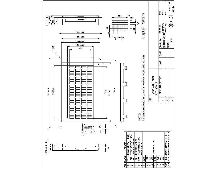
1.0 MECHANICAL SPECS
1. Overall Module Size
182.0mm(W) x 90.0mm(H) x max 13.0mm(D) for LED backlight
version
2. Dot Size
1.10mm(W) x 1.50mm(H)
3. Dot Pitch
1.20mm(W) x 1.60mm(H)
4. Duty
1/16
5. Controller IC
ST7066
6. LC Fluid
TN, STN
7. Polarizer
Reflective, Transflective, Transmissive
8. Viewing Angle
Bottom, Top
9. Backlight
Side LED
10. Temperature Range
Standard(0"C ~ 50"C), Wide(-20"C ~ 70"C)
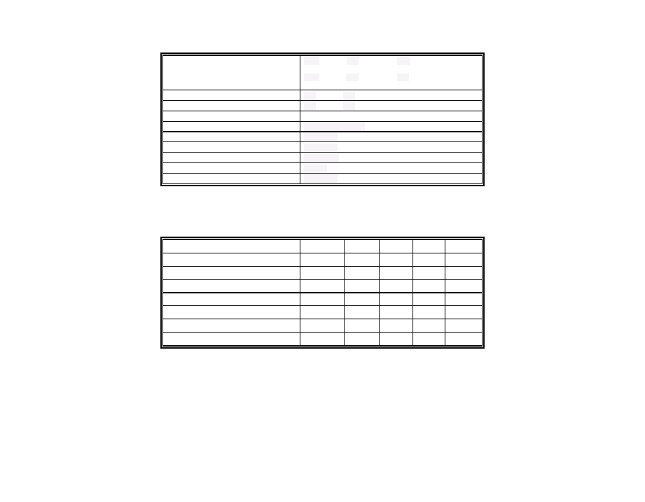
2.0 ABSOLUTE MAXIMUM RATINGS
Item
Symbol
Min
TypMax
Unit
Operating temperature (Standard)
Top
0
-
50
"C
Storage temperature (Standard)
Tst
-10
-
60
"C
Operating temperature (Wide temperature)
Top
-20
-
70
"C
Storage temperature (Wide temperature)
Tst
-30
-
80
"C
Input voltage
Vin
Vss
Vdd
V
Supply voltage for logic
Vdd- Vss
2.7
-
5.5
V
Supply voltage for LCD drive
Vdd- Vo
3.0
4.6
6.5
V
182.0mm(W) x 90.0mm(H) x max 9.50mm(D) for reflective
version
ACM2004E SERIES LCD MODULE
AZ DISPLAYS, INC. 04/24/02
2
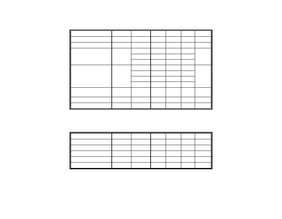
3.0 ELECTRICAL CHARACTERISTICS
Item
Symbol
Condition
Min
Typ
Max
Unit
Input voltage (high)
Vih
H level
2.2
-
Vdd
V
Input voltage (low)
Vil
L level
0
-
0.6
V
0ºC
-
4.8
5.4
25ºC
4.2
4.6
-
Recommended LC Driving
Voltage (Standard Temp)
Vdd - Vo
50ºC
3.9
4.3
-
V
-20ºC
-
6.4
7.2
0ºC
-
4.8
-
50ºC
-
4.3
-
Recommended LC Driving
Voltage (Wide Temp)
Vdd -Vo
70ºC
3.7
4.2
-
V
Power Supply Current
Idd
Vdd=5.0V,
fosc=270kHz
-
0.5
1.0
mA
LED Power Supply Voltage
Vfled
R=6.8
-
4.6
5.0
V
LED Power Supply Current
Ifled
R=6.8
-
240
480
mA
4.0 OPTICAL CHARACTERISTICS (Ta=25ºC, Vdd= 5.0V±0.25V, TN LC fluid)
Item
Symbol
Condition
Min
Typ
Max
Unit
Viewing angle (horizontal)
Cr
4.0
-25
-
-
deg
Viewing angle (vertical)
Cr
4.0
-30
-
30
deg
Contrast Ratio
Cr
=0
°
,
=0
°
-
2
-
Response time (rise)
Tr
=0
°
,
=0
°
-
120
150
ms
Response time (fall)
Tf
=0
°
,
=0
°
-
120
150
ms
ACM2004E SERIES LCD MODULE
AZ DISPLAYS, INC.
04/24/02 3
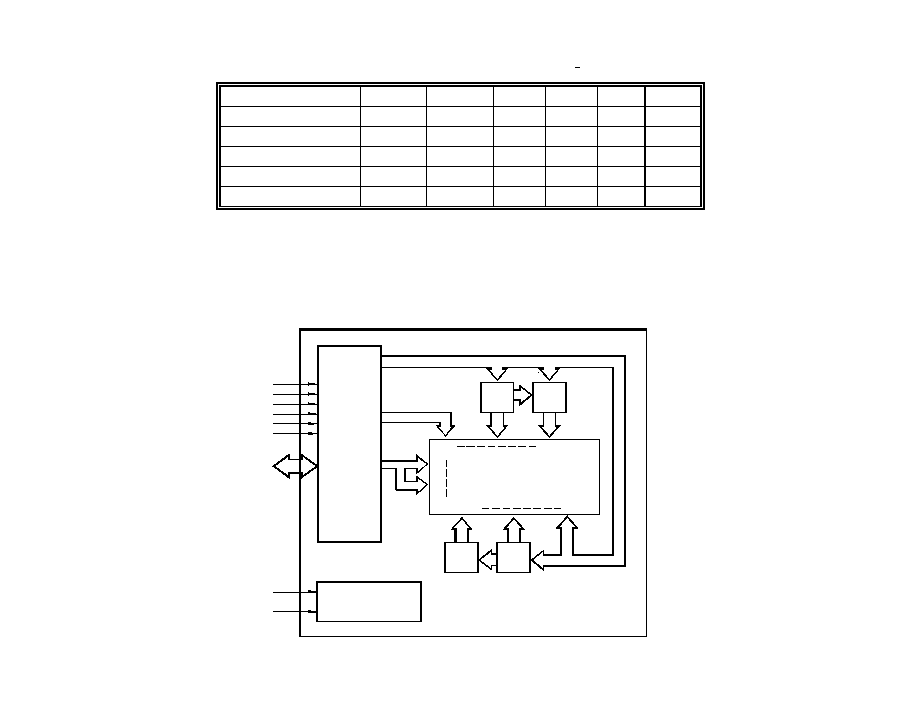
4.1 OPTICAL CHARACTERISTICS (Ta=25 C, Vdd= 5.0V 0.25V, STN LC fluid)
Item
Symbol
Condition
Min
Typ
Max
Unit
Viewing angle (horizontal)
Cr
2.0
-60
-
35
deg
Viewing angle (vertical)
Cr
2.0
-40
-
40
deg
Contrast Ratio
Cr
=0
°
,
=0
°
-
6
-
Response time (rise)
Tr
=0
°
,
=0
°
-
150
250
ms
Response time (fall)
Tf
=0
°
,
=0
°
-
150
250
ms
5.0 BLOCK DIAGRAM
LCD 20X4
U2
U1
SEG1- 40
SEG41- 80
SEG 1 SEG100
COM 16
8
LED BACKLIGHT
1. Vss
2. Vdd
3. Vo
4. RS
5. R/W
6. E
7. DB0
14. DB7
~
15/17 BL+
16/18 BL-
U3
SEG81-100
40
40
20
16
COM 1
COM32
16
SEG161- 200
40
U5
40
SEG121-160
U4
SEG 101 SEG200
20
SEG1- 40
SEG101-120
*
*Note: connected to Vss
o
+
ACM2004E SERIES LCD MODULE
AZ DISPLAYS, INC.
04/24/02
4
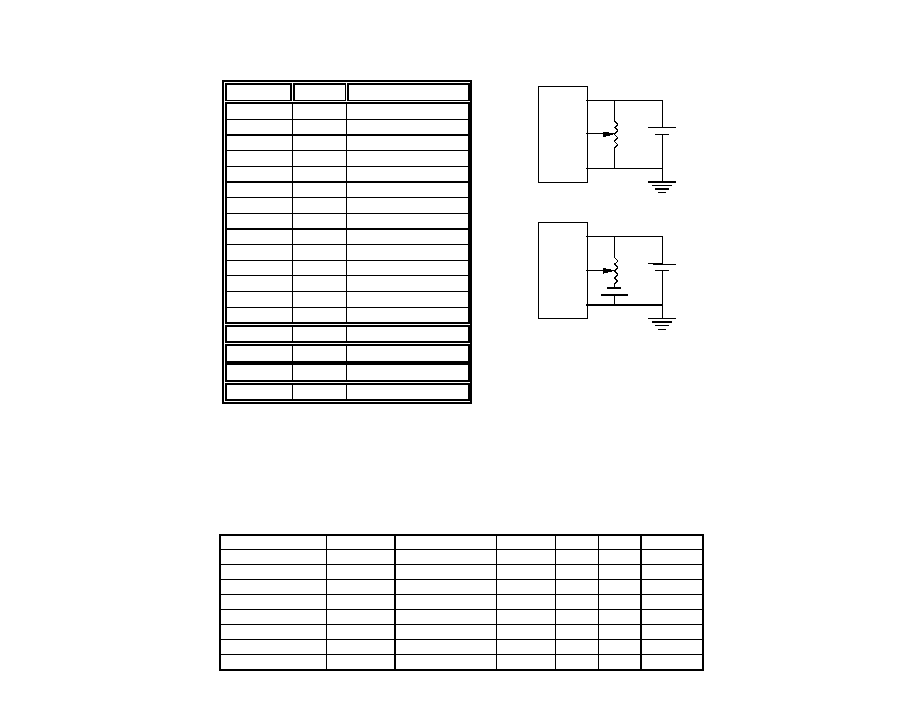
6.0 PIN ASSIGNMENT
7.0 POWER SUPPLY
Pin No.
Symbol
Function
1
Vss
Ground
2
Vdd
+5V
3
Vo
LCD contrast adjust
4
RS
Register select
5
R/W
Read / write
6
E
Enable
7
DB0
Data bit 0
8
DB1
Data bit 1
9
DB2
Data bit 2
10
DB3
Data bit 3
11
DB4
Data bit 4
12
DB5
Data bit 5
13
DB6
Data bit 6
14
DB7
Data bit 7
15
BL+
Power Supply for BL+
16
BL-
Power Supply for BL-
17
BL+
Power Supply for BL+
18
BL-
Power Supply for BL-
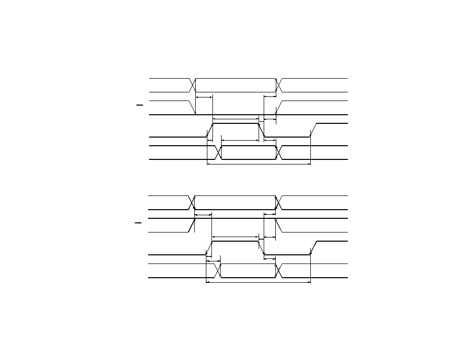
8.0 TIMING CHARACTERISTICS
Item
Symbol
Test Condition
Min.
Typ.
Max.
Unit
Enable cycle time
t
C
Fig. a, Fig. b
500
-
-
ns
Enable pulse width
t
W
Fig. a, Fig. b
220
-
-
ns
Enable rise/fall time
t
R
, t
F
Fig. a, Fig. b
-
-
25
ns
RS, R/W set up time
t
SU
Fig. a, Fig. b
40
-
-
ns
RS, R/W hold time
t
H
Fig. a, Fig. b
10
-
-
ns
Data delay time
t
D
Fig. b
-
-
120
ns
Data set up time
t
DSU
Fig. a
60
-
-
ns
Data hold time
t
DH
Fig. a, Fig. b
20
-
-
ns
Vss
Vo
Vdd
Vr
+5V
S
TANDARD TEMP RANGE
Vss
Vo
Vdd
Vr
+5V
W
IDE TEMP RANGE
-5V
Vr = 10K
~ 20K
*
*
*Note: connected to Vss
ACM2004E SERIES LCD MODULE
AZ DISPLAYS, INC. 04/24/02
5
V
IH1
V
IL1
V
IL1
IH1
IL1
V
V
V
IH1
V
IL1
V
IL1
V
IH1
IL1
V
V
IH1
IL1
V
Valid Data
t
SU
t
H
t
W
t
H
t
F
t
R
t
DSU
t
DH
t
C
RS
R/W
E
DB0~DB7
V
IL1
V
IH1
V
IL1
Fig. a Interface timing (data write)
V
IH1
V
IL1
V
IH1
IH1
IL1
V
V
V
IH1
V
IL1
V
IH1
V
IH1
IL1
V
V
IH1
IL1
V
Valid Data
t
SU
t
H
t
W
t
H
t
F
t
R
t
DSU
t
DH
t
C
RS
R/W
E
DB0~DB7
V
IL1
t
D
V
IH1
IL1
V
Fig. b Interface timing (data read)
AZ DISPLAYS, INC.
2.54 x 8 = 20.32
*
*Note: connected to Vss