AZ DISPLAYS, INC
.
Complete LCD Solutions
AZ DISPLAYS, INC. 1 1/15/02
ACM4004D SERIES LCD MODULE
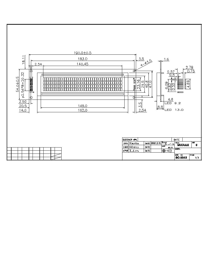
1.0 PHYSICAL DATA
Item Nominal Dimensions / Available Options Unit
Number of Characters
40 characters x 4 lines
-
Character Format
5 x 7 dots with cursor
-
Overall Module Size (W x H x D)
190.0 x 54.0 x max 13.0 for LED backlight version
190.0 x 54.0 x max 8.8 for reflective or EL backlight version
mm
Dot Size (W x H)
0.50 x 0.55
mm
Dot Pitch (W x H)
0.57 x 0.62
mm
Duty
1/16
-
Controller IC
KS0066
-
LC Fluid Options
TN, STN -
Polarizer Options
Reflective, Transflective, Transmissive
-
Backlight Options
EL, LED
-
Temperature Range Options
Standard, Wide temp
-
2.0 ABSOLUTE MAXIMUM RATINGS
Item Symbol Min Typ Max Unit
Operating temperature (Standard)
Top
0
-
50
°
C
Storage temperature (Standard)
Tst
-20
-
70
°
C
Operating temperature (Wide temp)
Top
-20
-
+70
°
C
Storage temperature (Wide temp)
Tst
-30
-
+80
°
C
Input voltage
V
I
V
SS
-
V
DD
V
Supply voltage for logic
V
DD
-V
SS
0
5.0
6.5
V
Supply voltage for LCD drive (Standard)
V
DD
-V
O
0
-
6.5
V
Supply voltage for LCD drive (Wide temp)
V
DD
-V
O
0
-
13.5
V
3.0 OPTICAL CHARACTERISTICS (Ta = 25C, VDD = 5.0V +/- 0.25V, STN Fluid)
Item Symbol Condition Min Typ Max Unit
Viewing angle (horizontal)
Cr
2.0
±
30
-
-
deg
Viewing angle (vertical)
Cr
2.0
-
40
-
deg
Contrast Ratio
Cr
=0
°
,
=0
°
-
3.0
-
Response time (rise)
Tr
=0
°
,
=0
°
-
120
240
ms
Response time (fall)
Tf
=0
°
,
=0
°
-
155
310
ms
AZ DISPLAYS, INC. 2
1/15/02
ACM4004D SERIES LCD MODULE
4.0 ELECTRICAL CHARACTERISTICS (Ta = 25C, VDD = 5.0V +/- 0.25V)
Item Symbol Condition Min Typ Max Unit
Supply voltage for LCD drive (Std temp)
V
DD
-V
O
Ta = 25
°
C
4.5
V
Supply voltage for LCD drive (Wide temp)
V
DD
-V
O
Ta = 25
°
C
6.2
V
Input voltage
V
I
-
4.75
5.0
5.25
V
Input high voltage
V
IH
-
0.8V
DD
-
V
DD
V
Input low voltage
V
IL
-
V
SS
-
V
Supply current
I
DD
V
DD
=5.0V
-
6.0
10.0 mA
LED power supply current
I
LED
Vf=4.2V
-
600
-
mA
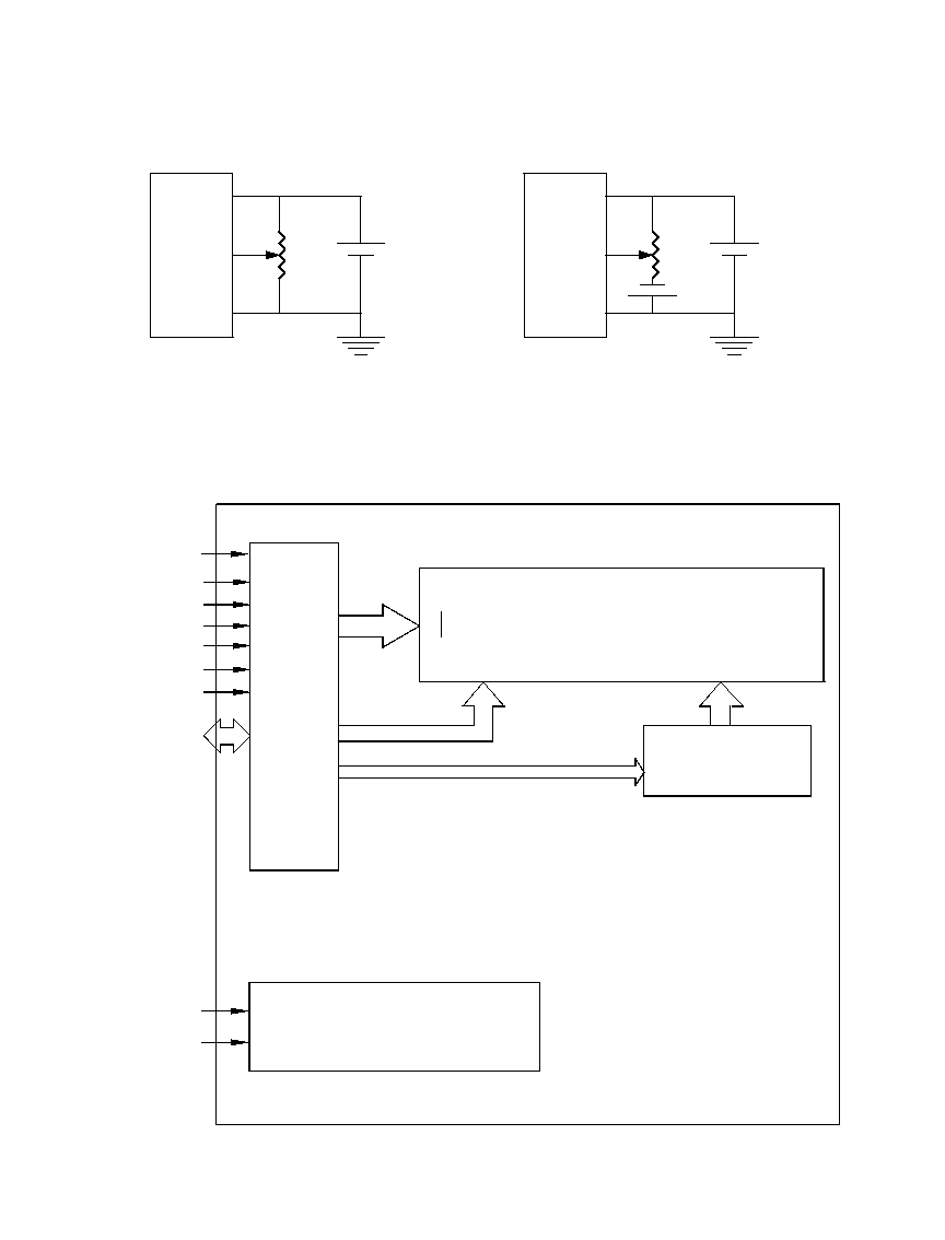
5.0 INTERFACE PIN CONNECTIONS
Pin No. Symbol Level Pin Description Function
1
DB7
Data bit 7
4-bit or 8-bit interface
2
DB6 H/L
Data bit 6
4-bit or 8-bit interface
3
V
O
-
By user
4
RS
H/L
H: Data; L: Instruction code
5
R/W
H/L
Read / write
H: Data read, L: Data write
6
E1
H, H
L
Start signal for data read/write
7
DB0
H/L
Data bit 0
8-bit interface
8
DB1
H/L
Data bit 1
8-bit interface
9
DB2
H/L
Data bit 2
8-bit interface
10
DB3
H/L
Data bit 3
8-bit interface
11
DB4
H/L
Data bit 4
4-bit or 8-bit interface
12
DB5
Data bit 5
4-bit or 8-bit interface
13
14
VSS
5V
Supply Voltage for logic
15
Anode for LED backlight
Power supply for LED/EL backlights
16
K
0V
Cathode for LED backlight
Power supply for LED/EL backlights
H/L
VDD
E2
Register Select
LCD Contrast Adjustment
0V
H, H
L
H/L
Enable for IC1
Ground
Enable for IC2
None
NC
-
No Connection
Start signal for data read/write
0V
5V
17
A
4.2V
18
0.2V
DD
AZ DISPLAYS, INC. 4 1/15/02
ACM4004D SERIES LCD MODULE
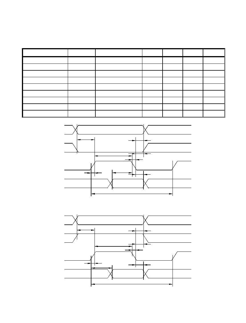
8.0 TIMING CHARACTERISTICS (KS0066 Controller)
Item
Symbol
Test Condition
Min.
Typ.
Max.
Unit
Enable cycle time
t
CYC
Fig. a, Fig. b
500
-
-
ns
Enable pulse width
PW
EH
Fig. a, Fig. b
220
-
-
ns
Enable rise/fall time
t
Er
, t
Ef
Fig. a, Fig. b
-
-
25
ns
RS, R/W set up time
t
AS
Fig. a, Fig. b
40
-
-
ns
RS, R/W hold time
t
H1
Fig. a, Fig. b
10
-
-
ns
Data set up time
t
DSW
Fig. a
60
-
-
ns
Data hold time
t
H2
Fig. a
10
-
-
ns
Data delay time
t
DDR
Fig. b
-
-
120
ns
Data hold time
t
H2
Fig. b
20
-
-
ns
0.6V -
0.6V -
2.2V -
DDR
- 0.6V
- 2.2V
Fig. b Interface timing (data read)
t
RS
R/W
E
DB0-DB7
RS
R/W
E
DB0-DB7
- 2.2V
- 0.6V
- 2.2V
- 0.6V
- 0.6V
- 2.2V
Ef
t
2.2V -
- 0.6V
2.2V -
EH
PW
AS
Er
t
0.6V -
- 2.2V
t
Fig. a Interface timing (data write)
Valid Data
Valid Data
CYC
t
- 0.6V
t
AS
EH
PW
0.6V -
Er
t
- 2.2V
- 0.6V
- 2.2V
CYC
t
2.2V -
0.6V -
H1
t
H1
t
H2
t
0.6V -
H1
2.2V -
t
0.6V -
H1
t
t
H2
Ef
t
2.2V -
DSW
t
0.6V -
2.2V -
- 0.6V