VEE-VSS
MAX 9.0
(D)mm
0.31
183.0
0.33
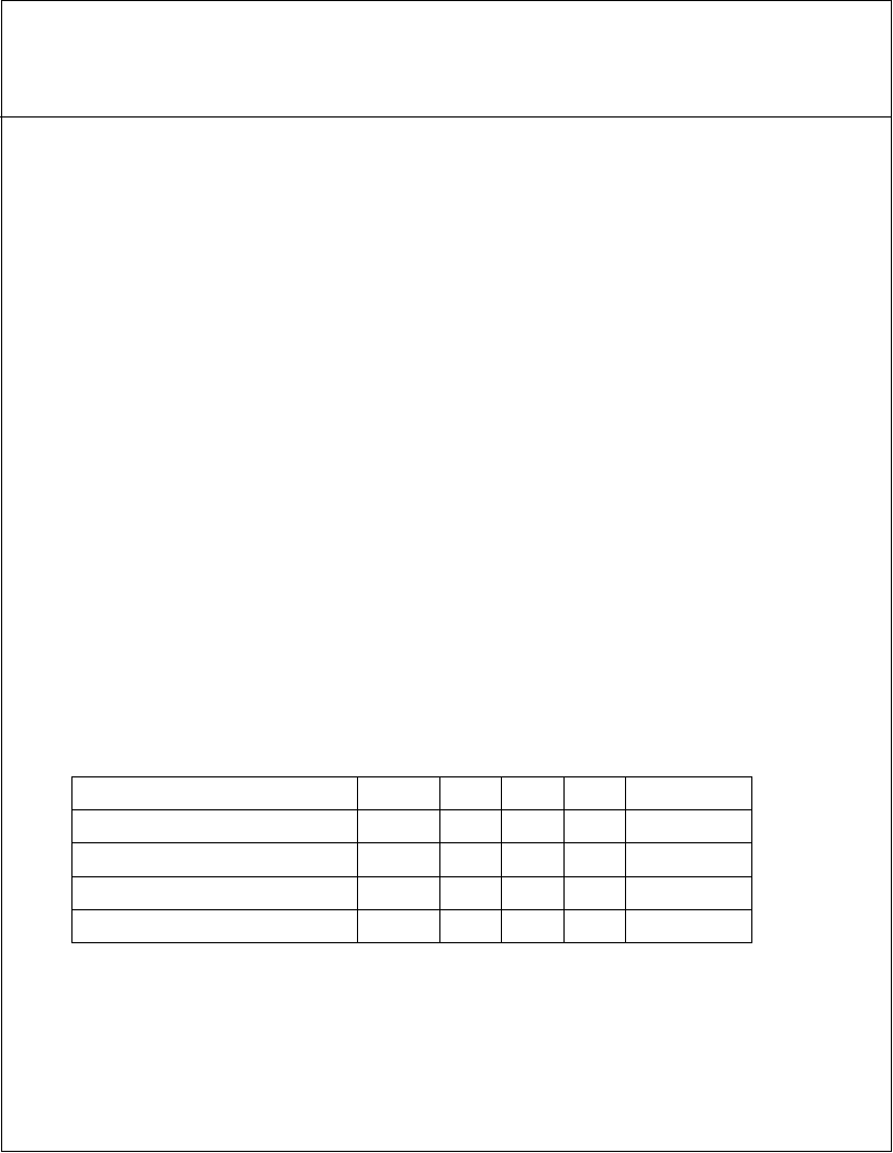
(H)mm
(H)mm
(W)mm x
(W)mm x
(W)mm x
(H)mm x
(6) Duty
(5) Number of Dots
(8) Viewing Direction
(9) Backlight
(4) Dot Pitch
(3) Dot Size
(2) Module Size
(1) Product No.
(10) Controller
(12) Weight
(13) Recommended CCFT Inverter
(11) DC/DC Converter
(7) LCD
0.11
0.09
CCFL
640 (W)xRGB x 480 (H)DOTS
6 0'clock
1/240
AGM6448V
264.0
495 g(approx.)
F-STN/Black and White(Normal Black/Negative Image)
CXA-L0612-VMR (TDK)
Without
Without
/Color Transmissive Type
2. ABSOLUTE MAXIMUM RATINGS
1. MECHANICAL DATA
AGM6448V Series LCD Module
Complete LCD Solutions
AZ DISPLAYS, INC.
PAGE 1 OF 8
Note 1
COMMENT
VSS=0V
V
-
V
V
UNIT
-
42.0
6.5
MAX
VDD+0.3
0
-
-0.3
-0.3
MIN
-
VI
SYMBOL
ITEM
Input Voltage
Power Supply for LCD Drive
Static Electricity
Power Supply for Logic
VDD-VSS
Note 1 LCM should be grounded during handling LCM.

Used lamp : Rating
Lamp power consumption
Lamp current
Lamp Voltage
(Normal Temp. LCM)
Supply Current for LCD
LCD Driving Voltage
Supply Current for Logic
Power Supply
Logic Circuit
Recommended
Input Voltage
S
L
Y
F
V
X
L
L
L
B
L
Lu
SYMBOL
PARAMETER
Starting voltage
Lamp life time
Lamp frequcncy
Brightness
Color Cooridinates
Luminance Uniformity
LCM : Rating
Surface Luminance
(*2) Power consumption excludes inverter loss .
CCFT backlight may least affect the display quality .
(*1) It is recommended that I be not more than 5.0 mArms so that heat radiation of
8.0
22.8
18.8
23.5
24.1
5.0
TYP.
a
White
T =25�C
REMARK
2
kHz
-
hrs
2
%
UNIT
-
-
-
0.31
600
0.31
-
-
MAX.
Vrms
cd/m
cd/m
-
-
-
0.29
35
0.29
TYP.
85
76
0.27
10000
22000
-
-
0.27
MIN.
-
-
VIH
VIL
VDD-VSS
SYMBOL
IEE
IDD
L
L
L
I
P
V
SYMBOL
VEE-VSS
ITEM
PARAMETER
3.2 ELECTRICAL CHARACTERISTICS OF BACKLIGHT
3.1 ELECTRICAL CHARACTERISTICS OF LCM
3. ELECTRICAL CHARACTERISTICS
PAGE 2 OF 8
V
V
V
0.2VDD
5.5
VDD
MAX.
V
mA
mA
-
REMARK
(*1)
(*2)
24.2
23.0
23.6
12.5
28.5
UNIT
-
-
4.5
0.8VDD
0
MIN.
W
UNIT
6
-
MAX.
mArms
Vrms
-
22.6
23.3
-
-
Ta= 25�C
L level
H level
CONDITION
5
TYP.
2.7
535
-
MIN.
4
-
Duty=1/240
Bias=1/13
VDD=5.0V
Ta= 25�C
0�C
50�C
VEE-VSS = 23.5V
VDD-VSS = 5.0V
25�C
Complete LCD Solutions
AZ DISPLAYS, INC.

Power supply voltage for LCD (+)
Power supply voltage for LCD (+)
GND
GND
+5V
Display data for lower column driver
Display data for lower column driver
Display data for lower column driver
Display data for lower column driver
Display data for lower column driver
Display data for lower column driver
Display data for lower column driver
Display data for lower column driver
Display data for upper column driver
Display data for upper column driver
Display data for upper column driver
Display data for upper column driver
Display data for upper column driver
Display data for upper column driver
Display data for upper column driver
Display data for upper column driver
GND
Clock signal for shifting the serial data.
GND
shift registers.
The CL1 latches the serial data in the
H ---display ON, L --display OFF
each display cycle.
The FLM signal indicates the beging of
N.C
GND
N.C
SYMBOL
CN1:15PIN MOLEX 53261-1590
VSS
CL1
LD0
LD2
LD3
LD1
UD7
UD6
UD5
UD4
UD3
4
5
6
7
8
9
10
12
14
13
16
17
18
19
15
CN3
11
DISPOFF
LCM
CN3:30PIN JAE/IL-402-30S-S1L-SA
INTERFACE
VEE
VSS
VSS
VDD
LD5
LD6
LD7
LD4
1
PIN NO.
VEE
NC
VEE
21
20
23
22
25
24
27
26
29
30
INTERFACE
28
FLCN1:MITSUMI/M63M83-04
3
FLCN1
CFL
2
(Suitable Connecter:MITSUMI/M60-04-30-134P or M60-04-30-114P or M61M73-04)
Power supply voltage for LCD (+)
4
Power supply voltage for CFL
HV
1
3
2
PIN NO.
4
5
6
7
8
9
10
12
14
13
1
2
3
4
15
11
CN1
FUNCTION
CN2:14PIN MOLEX 53261-1490
5
6
7
8
9
10
12
11
14
13
CN2
FUNCTION
-
CFL GND
-
SYMBOL
NC
FLM
1
3
2
PIN NO.
CL2
UD2
UD1
UD0
VSS
6.INTERFACE PIN CONNECTION
PAGE 5 OF 8
Complete LCD Solutions
AZ DISPLAYS, INC.

