
PA050XS1
The information contained herein is the exclusive property of Prime View International Co., Ltd. and shall not be distributed,
reproduced, or disclosed in whole or in part without prior written permission of Prime View International Co., Ltd.
PAGE:1
Version : 1.6
TECHNICAL SPECIFICATION
MODEL NO. : PA050XS1
Customer's Confirmation
Customer
Date
By
PVI's Confirmation
Confirmed By
Prepared By
FOR MORE INFORMATION:
AZ DISPLAYS, INC.
75 COLUMBIA, ALISO VIEJO, CA, 92656
http://www.
AZDISPLAYS.com
Date : Jul. 15, 2004
This technical specification is subject to change without notice.
Please return 1 copy with your signature on this page for approval.

PA050XS1
The information contained herein is the exclusive property of Prime View International Co., Ltd. and shall not be distributed,
reproduced, or disclosed in whole or in part without prior written permission of Prime View International Co., Ltd.
PAGE:2
TECHNICAL SPECIFICATION
CONTENTS
NO. ITEM PAGE
- Cover
(PA050XS1) 1
- Contents 2
1 Application 3
2 Features 3
3 Mechanical
Specifications 3
4
Mechanical Drawing of TFT-LCD module
4
5
Input / Output Terminals
5
6
Pixel Arrangement and input connector pin NO.
7
7
Absolute Maximum Ratings
8
8 Electrical
Characteristics 8
9
Power On Sequence
18
10 Optical
Characteristics 18
11 Handling
Cautions 22
12 Reliability
Test 23
13
Indication of Lot Number Label
23
14 Block
Diagram 24
15 Packing 25
- Revision
History 26

PA050XS1
The information contained herein is the exclusive property of Prime View International Co., Ltd. and shall not be distributed,
reproduced, or disclosed in whole or in part without prior written permission of Prime View International Co., Ltd.
PAGE:3
1. Application
This technical specification applies to 5" color TFT-LCD module , PA050XS1. The applications of the
panel are car TV, portable DVD, GPS, multimedia applications and others AV system..
2. Features
. Compatible with NTSC & PAL system
. Pixel in stripe configuration
. Slim and compact
. Image Reversion : Up/Down and Left/Right
3. Mechanical Specifications
Parameter Specifications
Unit
Screen Size
5 (diagonal)
inch
Display Format
960◊234
dot
Active Area
102.72(H)◊ 74.53(V)
mm
Dot Pitch
0.107 (H)◊ 0.319 (V)
mm
Pixel Configuration
Stripe
Outline Dimension
119.3(W)◊ 91.4(H)◊ 7.5(D)(typ.)
mm
Surface Treatment
Anti - Glare
Weight
124±5
g

PA050XS1
The information contained herein is the exclusive property of Prime View International Co., Ltd. and shall not be distributed,
reproduced, or disclosed in whole or in part without prior written permission of Prime View International Co., Ltd.
PAGE:4
4. Mechanical Drawing of TFT-LCD Module
PA050XS1
The information contained herein is the exclusive property of Prime View International Co., Ltd. and shall not be distributed,
reproduced, or disclosed in whole or in part without prior written permission of Prime View International Co., Ltd.
PAGE:5
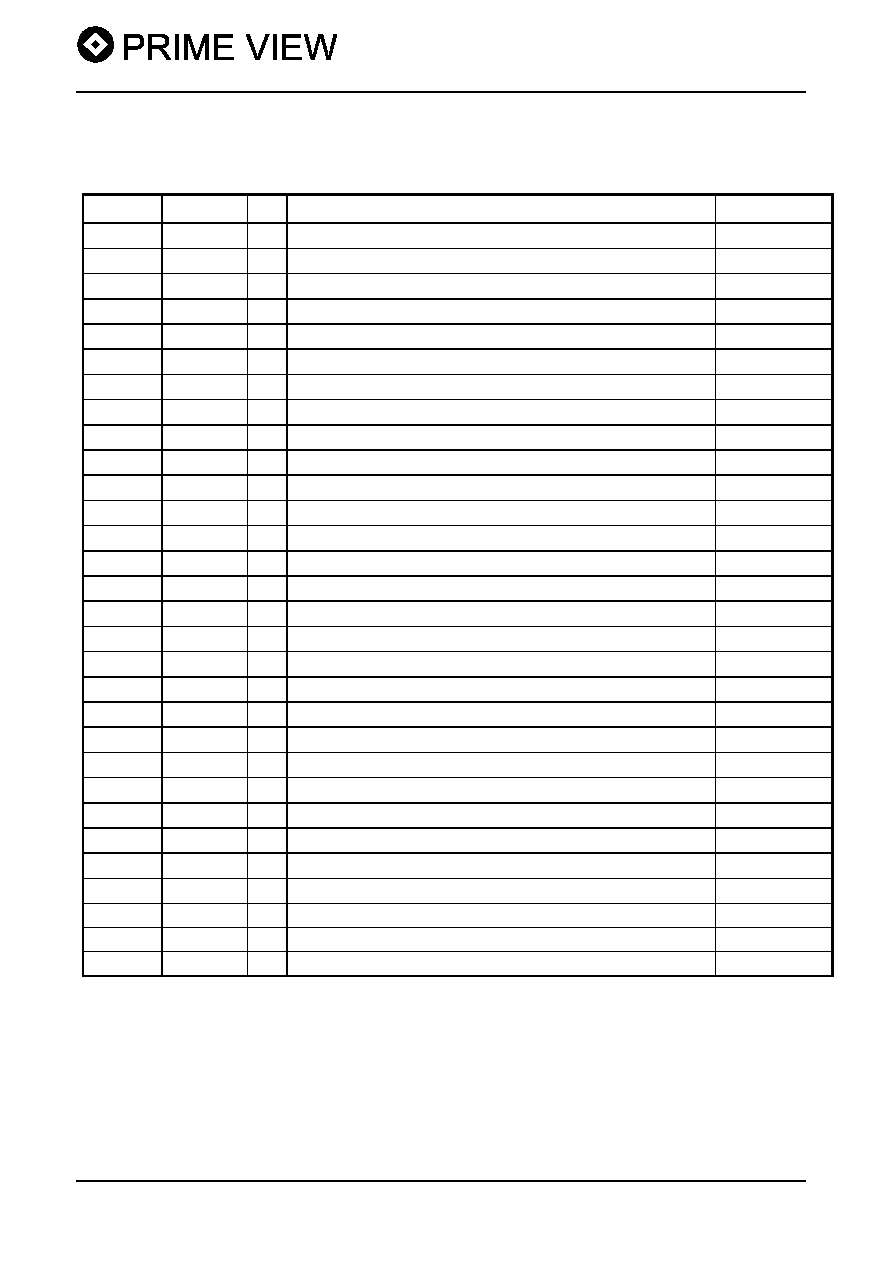
5. Input / Output Terminals
TFT-LCD Module Connector
FPC Down Connect , 30Pins , Pitch : 0.5 mm
Pin No
Symbol
I/O
Description
Remark
1
DIO1
I/O
Vertical start pulse
Note 5 ≠ 5
2
CPV
I
Shift clock for gate driver
3
VGL
I
Power for gate driver (AC voltage)
Note 5 - 1
4 NC
-
No
connection
5
VEE
I
Negative power for gate driver (DC voltage)
Note 5 - 2
6 NC
-
No
connection
7
XOE
I
Output enable for gate driver
8
VSS
-
Ground for digital circuit
9
VCC
I
Supply voltage for logic control circuit for gate driver
Note 5 - 3
10 NC
-
No
connection
11
VGH
I
Positive power for gate driver
Note 5 - 4
12 NC
-
No
connection
13
U/D
I
Up/Down control for gate driver
Note 5 ≠ 5
14
DIO2
I/O
Vertical start pulse
Note 5 ≠ 5
15
VCOM
I
Common electrode voltage
Note 5 ≠ 1
16
STH1
I/O
Start pulse for source driver
Note 5 ≠ 5
17
VDD1
I
Supply power for digital circuit
Note 5 ≠ 3
18
VSS1
-
Ground for digital circuit
19
VDD2
I
Supply power for analog circuit
Note 5 ≠ 3
20
VSS2
-
Ground for analog circuit
21
R/L
I
Left/Right control for source driver
Note 5 ≠ 5
22
VR
I
Video input R
Note 5 ≠ 1
23
VG
I
Video input G
Note 5 ≠ 1
24
VB
I
Video input B
Note 5 ≠ 1
25
CPH1
I
Sampling and shift clock for source driver
26
CPH2
I
Sampling and shift clock for source driver
27
CPH3
I
Sampling and shift clock for source driver
28
STH2
I/O
Start pulse for source driver
Note 5 ≠ 5
29
OEH
I
Output enable for source driver
30 NC
-
No
connection
Note 5 ≠ 1 : V
COM
= 6V
PP
.