
PA080XS1
The information contained herein is the exclusive property of Prime View International Co., Ltd. and shall not be distributed,
reproduced, or disclosed in whole or in part without prior written permission of Prime View International Co., Ltd.
PAGE:1
Version : 0.2
TECHNICAL SPECIFICATION
MODEL NO. : PA080XS1
Customer's Confirmation
Customer
Date
By
PVI's Confirmation
Confirmed By
Prepared By
FOR MORE INFORMATION:
AZ DISPLAYS, INC.
75 COLUMBIA, ALISO VIEJO, CA, 92656
http://www.
AZDISPLAYS.com
Date : Mar.22,2005
This technical specification is subject to change without notice.
Please return 1 copy with your signature on this page for approval.
PA080XS1
The information contained herein is the exclusive property of Prime View International Co., Ltd. and shall not be distributed,
reproduced, or disclosed in whole or in part without prior written permission of Prime View International Co., Ltd.
PAGE:2
TECHNICAL SPECIFICATION
CONTENTS
NO. ITEM PAGE
- Cover 1
- Contents 2
1 Application 3
2 Features 3
3 Mechanical
Specifications 3
4
Mechanical Drawing of TFT-LCD module
4
5
Input / Output Terminals
5
6
Pixel Arrangement and input connector pin NO.
6
7
Absolute Maximum Ratings
6
8 Electrical
Characteristics 7
9 Power
Sequence 17
10 Optical
Characteristics 17
11 Handling
Cautions 21
12 Reliability
Test 22
13 Block
Diagram 23
14 Packing 24
-
Revision History
25

PA080XS1
The information contained herein is the exclusive property of Prime View International Co., Ltd. and shall not be distributed,
reproduced, or disclosed in whole or in part without prior written permission of Prime View International Co., Ltd.
PAGE:3
1. Application
This technical specification applies to 8" color TFT-LCD module, PA080XS1. The applications
of the panel are car TV, portable DVD, GPS, multimedia applications and others AV system.
2. Features
. Pixel in stripe configuration
. Slim and compact
. High Brightness
. Image Reversion
Up/Down and Left/Right
. Column inversion driving
3. Mechanical Specifications
Parameter Specifications
Unit
Screen Size
8(diagonal)
Inch
Display Format
1440
�
468
dot
Active Area
161.28 (H)
�
117.94 (V)
mm
Dot Pitch
0.112(H)
�
0.252(V)
mm
Pixel Configuration
Stripe
Outline Dimension
172.4(W)
�
131.99(H)
�
6.64(D)(typ.)
mm
Surface Treatment
Anti-Glare
Weight
TBD
g

PA080XS1
The information contained herein is the exclusive property of Prime View International Co., Ltd. and shall not be distributed,
reproduced, or disclosed in whole or in part without prior written permission of Prime View International Co., Ltd.
PAGE:5
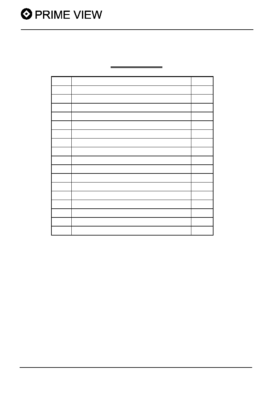
5. Input / Output Terminals
LCD Module Connector
FPC Down Connect , 32 Pins , Pitch : 0.5 mm
Pin No Symbol I/O
Description
Remark
1
STH2 I/O
Start pulse for source driver
Note 5-2
2
OEH
I
Output enable for source driver
3
POL
I
P0larity control for column inversion
4
MOD
I
Simultaneous/sequential mode select
5
R/L
I
Left / Right Control for source driver
Note 5-2
6
V
DD1
-
Supply voltage of logic circuit for source driver
7
CPH3
I
Sample and shift clock for source driver
8
CPH2
I
Sample and shift clock for source driver
9
CPH1
I
Sample and shift clock for source driver
10
V
SS1
-
Ground of logic circuit for source driver
11
V
DD2
-
Supply voltage of analog circuit for source driver
12
VB-
I
Video input B for negative polarity
13
VG-
I
Video input G for negative polarity
14
VR-
I
Video input R for negative polarity
15
V
SS2
-
Ground for analog circuit for source driver
16
VB+
I
Video input B for positive polarity
17
VG+
I
Video input G for positive polarity
18
VR+
I
Video input R for positive polarity
19
V
SS2
-
Ground for analog circuit for source driver
20
STH1 I/O
Start pulse for source driver
Note 5-2
21
V
COM
I
Voltage for common electrode
22
OE1
I
Output enable for gate driver
23
OE2
I
Output enable for gate driver
24
OE3
I
Output enable for gate driver
25
U/D
I
Up / Down Control for gate driver
Note 5-1
26
CKV
I
Shift clock for gate driver
27
STVD I/O
Vertical start pulse
Note 5-1
28
STVU I/O
Vertical start pulse
Note 5-3
29
V
CC
-
Power supply for gate driver circuit
30
V
EE
-
Negative power gate driver
Note 5-4
31
V
GH
-
Positive power gate driver
Note 5-5
32
GND
-
Ground for gate driver
Note 5-1
U/D STVD STVU scanning
direction
Vcc Input output
up
todown
GND Output
input
down to up
Note 5-2
R/L STH1 STH2 scanning
direction
Vcc
input
output
left to right
GND output
input
right to left
The definitions of Note 5-1,5-2
