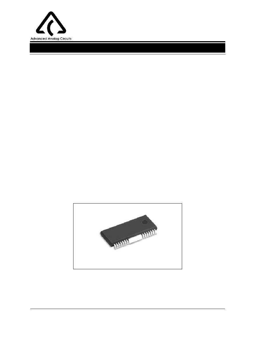
5-CHANNEL MOTOR DRIVER FOR DVD PLAYER AM5665
Preliminary Datasheet
1
Apr. 2005 Rev. 1. 1
BCD Semiconductor Manufacturing Limited
General Description
The AM5665 is a 5-channel BTL driver IC, in which
two channels drive DC motor, two channels with cur-
rent feedback drive the coils, such as the focus and the
tracking actuator of DVD player, and the other one
channel drives the bi-direction DC motor for tray.
The AM5665 is available in standard HSOP-28 pack-
age.
Features
∑
2-Channel DC Motor BTL Driver
∑
2-Channel BTL Driver for Coils with Current
Feedback
∑
1-Channel Forward/Reverse Control DC Motor
Driver
∑
Built-in Thermal Shutdown Circuit
∑
Built-in Standby Circuit
∑
Operating Voltage: 4.5 to 8.0V
Applications
∑
DVD Player
Figure 1. Package Type of AM5665
HSOP-28
5-CHANNEL MOTOR DRIVER FOR DVD PLAYER AM5665
Preliminary Datasheet
2
Apr. 2005 Rev. 1. 1
BCD Semiconductor Manufacturing Limited
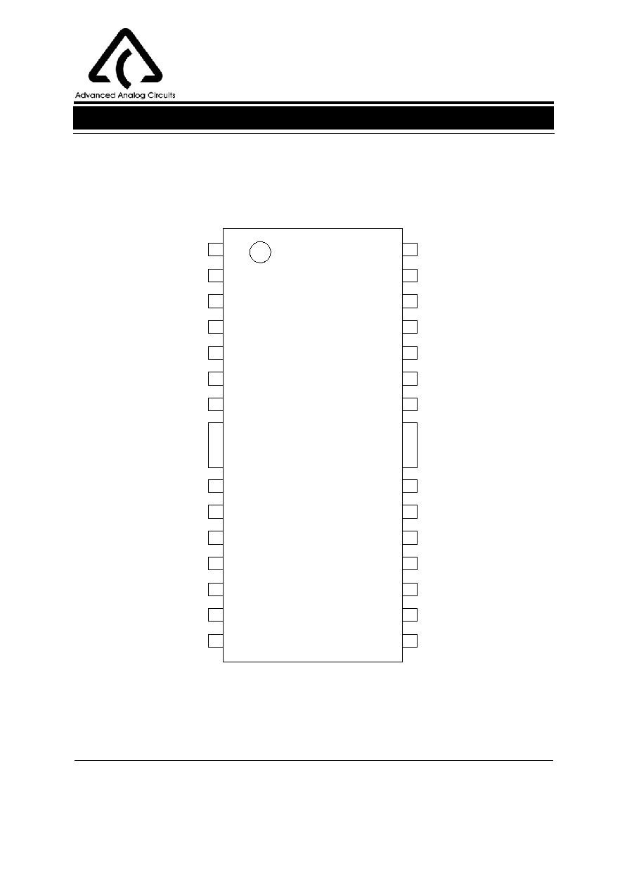
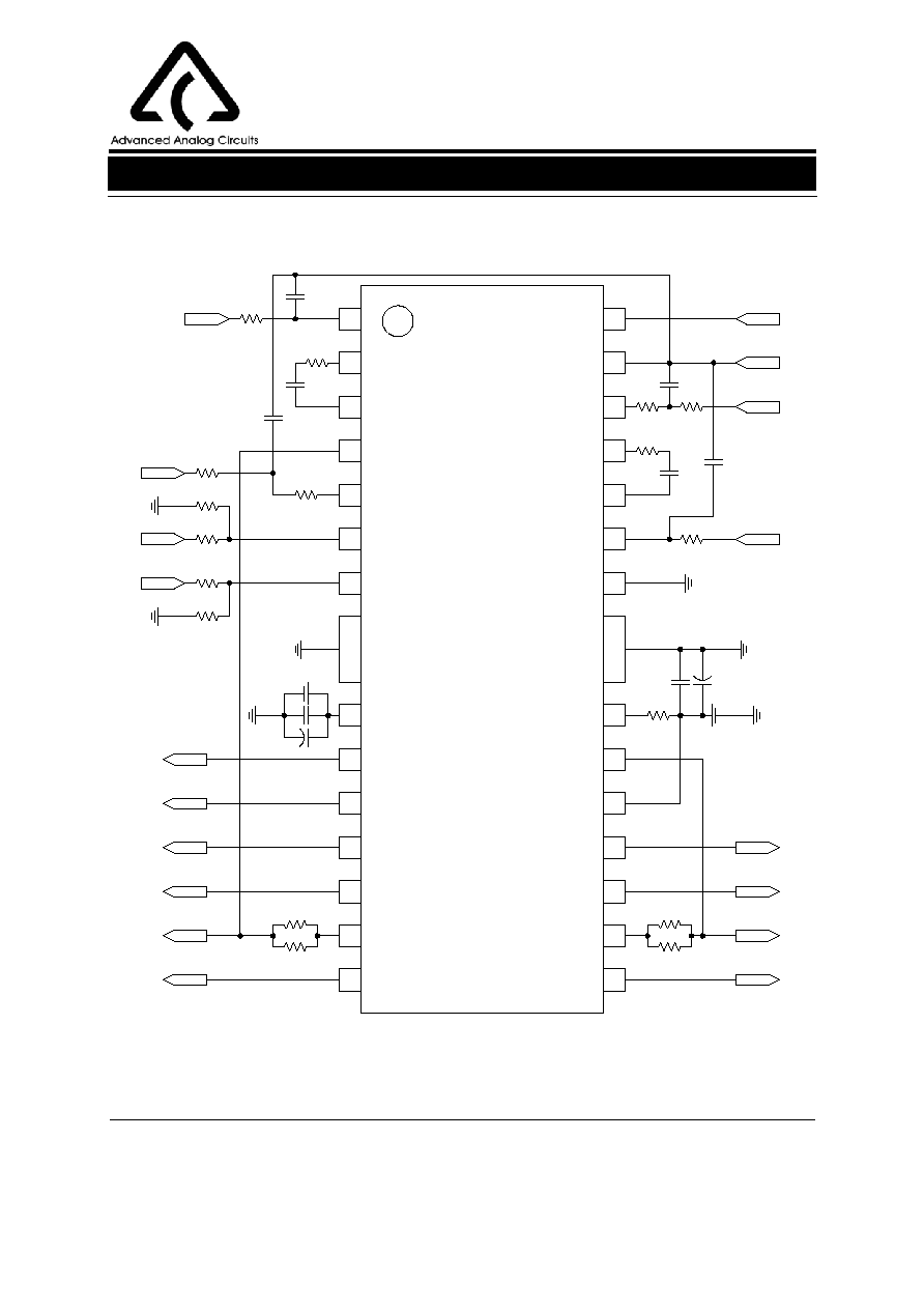
Pin Configuration
Figure 2. Pin Configuration of AM5665 (Top View)
M Package
(
HSOP-28
)
2
9
10
11
12
13
14
8
6
1
3
4
5
7
28
27
26
25
24
23
22
21
20
19
18
17
15
16
STBY
V
BIAS
V
IN
TK
CTKerr1
CTKerr2
V
IN
LD
GND
VCTL
VNFTK
V
CC2
VOLD-
VOLD+
VOTK-
VOTK+
V
IN
FC
CFCerr1
CFCerr2
VNFFC
V
IN
SL
FWD
REV
V
CC1
VOTR-
VOTR+
VOSL-
VOSL+
VOFC-
VOFC+
PGND
PGND
5-CHANNEL MOTOR DRIVER FOR DVD PLAYER AM5665
Preliminary Datasheet
3
Apr. 2005 Rev. 1. 1
BCD Semiconductor Manufacturing Limited
Pin Description
Pin Number
Pin Name
Function
1
V
IN
FC
Focus driver input
2
CFCerr1
Capacitor connection 1 for the error amp filter of focus channel
3
CFCerr2
Capacitor connection 2 for the error amp filter of focus channel
4
VNFFC
Focus driver feedback pin
5
V
IN
SL
Sled driver input
6
FWD
Tray driver forward input
7
REV
Tray driver reverse input
8
V
CC1
Power supply 1
9
VOTR-
Tray driver output (-)
10
VOTR+
Tray driver output (+)
11
VOSL-
Sled driver output (-)
12
VOSL+
Sled driver output (+)
13
VOFC-
Focus driver output (-)
14
VOFC+
Focus driver output (+)
15
VOTK+
Tracking driver output (+)
16
VOTK-
Tracking driver output (-)
17
VOLD+
Loading driver output (+)
18
VOLD-
Loading driver output (-)
19
V
CC2
Power supply 2
20
VNFTK
Tracking driver feedback pin
21
VCTL
Tray driver speed control pin
22
GND
Ground
23
V
IN
LD
Loading driver input
24
CTKerr2
Capacitor connection 2 for the error amp filter of tracking channel
25
CTKerr1
Capacitor connection 1 for the error amp filter of tracking channel
26
V
IN
TK
Tracking driver input
27
V
BIAS
VREF input pin
28
STBY
Stand-by control
5-CHANNEL MOTOR DRIVER FOR DVD PLAYER AM5665
Preliminary Datasheet
4
Apr. 2005 Rev. 1. 1
BCD Semiconductor Manufacturing Limited
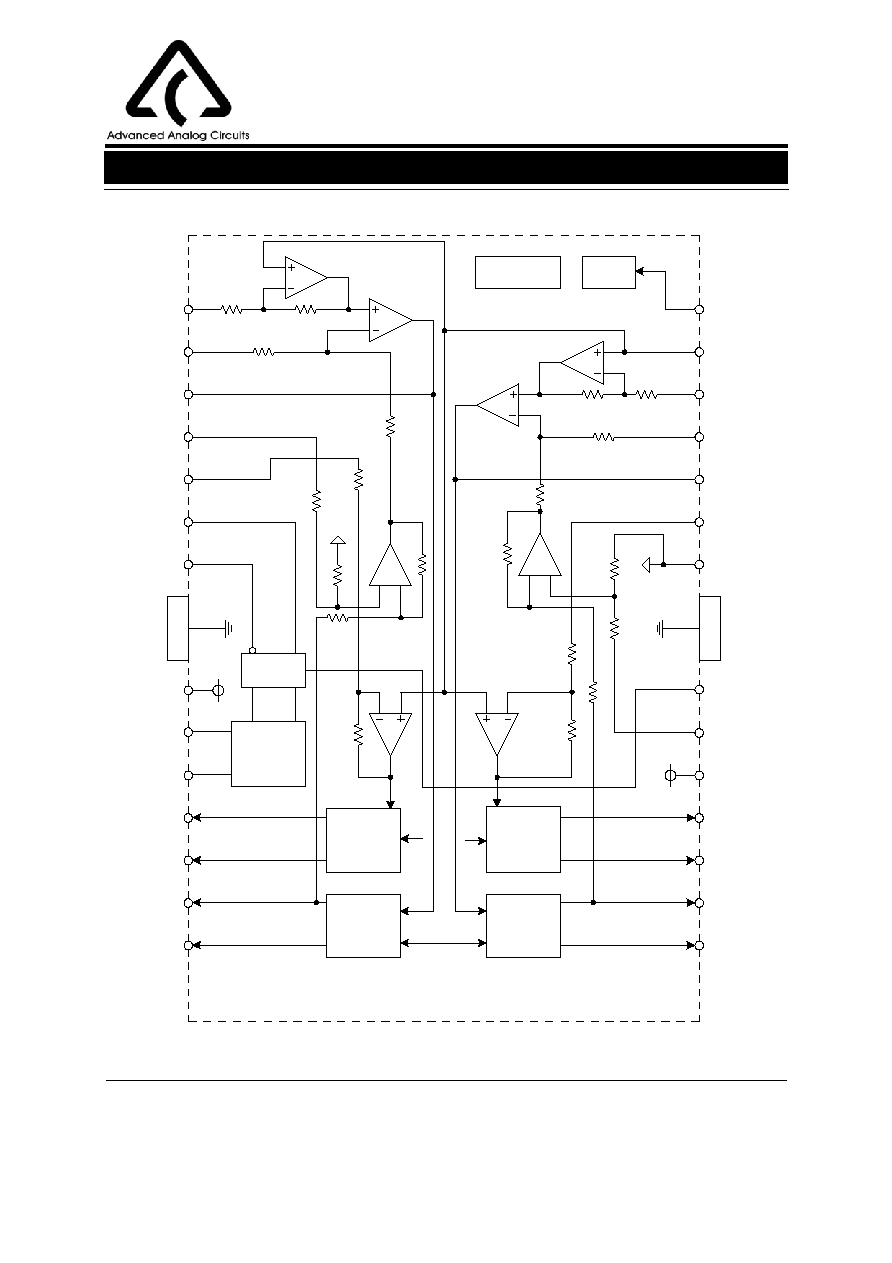
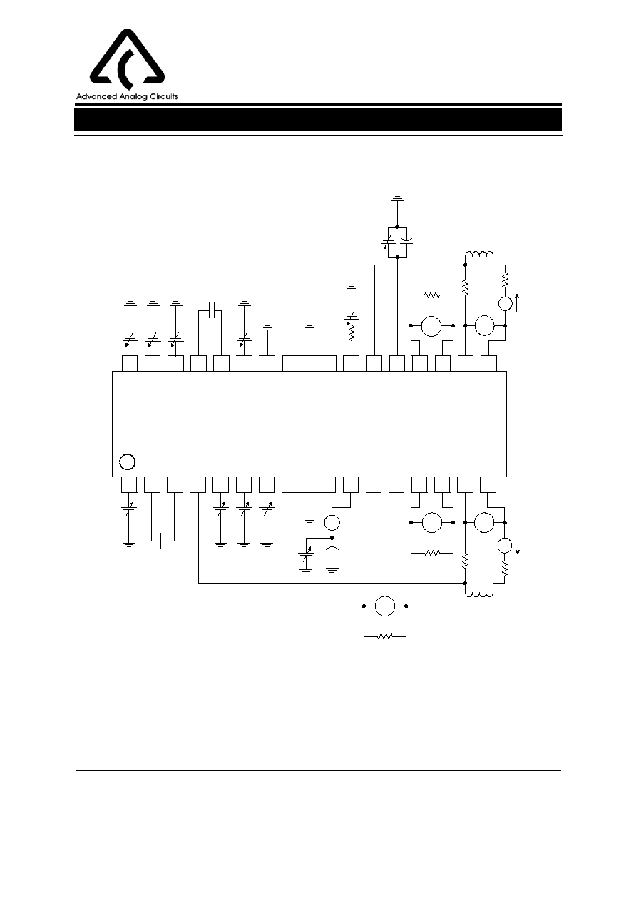
Functional Block Diagram
Figure 3. Functional Block Diagram of AM5665
7.5K
20K
10K
20k
25K
SLED
DRIVER
ACTUATOR
DRIVER
20k
10k
7.5k
7.5k
LOADING
DRIVER
ACTUATOR
DRIVER
20k
10k
20k
STBY
V
BIAS
V
IN
TK
CTKerr1
CTKerr2
V
IN
LD
GND
VCTL
VNFTK
V
CC2
VOLD-
VOLD+
VOTK-
VOTK+
V
IN
FC
CFCerr1
CFCerr2
VNFFC
V
IN
SL
FWD
REV
V
CC1
VOTR-
VOTR+
VOSL-
VOSL+
VOFC-
VOFC+
1
2
3
4
5
6
7
8
9
10
11
12
13
14
15
16
17
18
19
20
21
22
23
24
25
26
27
28
STAND-
BY
THERMAL
SHUT DOWN
10K
10k
V
CC1
V
CC2
V
CC1
7.5k
15k
20k
10k
TRAY
DRIVER
Pre-DRV
10k
PGND
PGND
10k
◊
2
◊
2
V
CC2
V
CC
1
5-CHANNEL MOTOR DRIVER FOR DVD PLAYER AM5665
Preliminary Datasheet
5
Apr. 2005 Rev. 1. 1
BCD Semiconductor Manufacturing Limited
Ordering Information
Absolute Maximum Ratings (Note 1)
Recommended Operating Conditions
Parameter Symbol
Value
Unit
Supply Voltage
V
CC1, 2
9.6
V
ESD (HBM)
ESD
2000
V
Power Dissipation
P
D
1.7
W
Storage Temperature Range
T
STG
-55 to +150
Parameter
Symbol
Min
Max
Unit
Supply Voltage
V
CC1
4.5
8.0
V
V
CC2
4.5 to V
CC1
V
Operating Temperature
T
A
0
70
Note 1: Stresses greater than those listed under "Absolute Maximum Ratings" may cause permanent damage to
the device. These are stress ratings only, and functional operation of the device at these or any other conditions
beyond those indicated under "Recommended Operating Conditions" is not implied. Exposure to "Absolute Max-
imum Ratings" for extended periods may affect device reliability.
Package
Temperature
Range
Part Number
Marking ID
Packing
Type
Tin Lead
Lead Free
Tin Lead
Lead Free
HSOP-28
0 to 70
o
C
AM5665M28
AM5665M28-E1
AM5665M28
AM5665M28-E1
Tube
BCD Semiconductor's Pb-free products, as designated with "E1" suffix in the part number, are RoHS compliant.
Circuit Type
Package
M28: HSOP-28
E1: Lead Free
Blank: Tin Lead
AM5665
-

5-CHANNEL MOTOR DRIVER FOR DVD PLAYER AM5665
Preliminary Datasheet
6
Apr. 2005 Rev. 1. 1
BCD Semiconductor Manufacturing Limited
Electrical Characteristics
Parameter
Symbol
Conditions
Min
Typ
Max
Unit
Quiescent Current
I
CC
No load
18
27
mA
Standby Current
I
ST
2.3
4.0
mA
Standby on Voltage
V
STON
0
0.5
V
Standby off Voltage
V
STOFF
2.0
5.0
V
Actuator Driver
Output Offset Current
I
OO1,2
-10
+10
mA
Maximum Output Voltage
V
O1,2MAX
V
IN
=V
BIAS
±
1.5V
3.3
3.5
V
Transmission Gain
gm
V
IN
=V
BIAS
±
0.2V
1.3
1.5
1.7
A/V
Sled Motor Driver
Output Offset Voltage
V
OOSL
-100
100
mV
Maximum Output Voltage
V
O3MAX
V
IN
=V
BIAS
±
1.5V
3.3
3.5
V
Closed-Loop Voltage Gain
G
VSL
V
IN
=V
BIAS
±
0.2V
18.0
20.0
22.0
dB
Loading Motor Driver
Output Offset Voltage
V
OOLD
-50
50
mV
Maximum Output Voltage
V
O4MAX
V
IN
=V
BIAS
±
5.5V
3.3
3.5
V
Closed-Loop Voltage Gain
G
VLD
V
IN
=V
BIAS
±
0.2V
14
16
18
dB
Gain Error by Polarity
G
VLD
0
1
2
dB
Tray Motor Driver
Output Offset Voltage
V
OOTR
R
L5
=45
, R
VCTL
=0
-50
0
50
mV
Maximum Output Voltage
V
O5MAX1
R
L5
=45
, R
VCTL
=400
1.3
1.5
1.7
V
V
O5MAX2
R
L5
=45
, R
VCTL
=0
3.8
4.0
4.2
V
Input High Level Voltage
V
IH
2.0
5.0
V
Input Low Level Voltage
V
IL
0
0.8
V
(T
A
=25
o
C
, V
CC1
=V
CC2
=5V, V
BIAS
=1.65V, R
L1
=R
L2
=8
, R
L3
=R
L4
=12
, R
L5
=45
, unless otherwise specified.)
5-CHANNEL MOTOR DRIVER FOR DVD PLAYER AM5665
Preliminary Datasheet
7
Apr. 2005 Rev. 1. 1
BCD Semiconductor Manufacturing Limited
Test Circuit
Figure 4. Test Circuit of AM5665
28
25
22
23
24
26
27
15
16
17
18
19
20
21
1
4
7
6
5
3
2
14
13
12
11
10
9
8
V
O4
R
L4
0.5
V
O1
A
R
L1
0.5
V
O2
A
R
L2
V
O3
R
L3
A
100
µ
H
100
µ
H
-
+
-
+
+
-
-
+
+
-
+
-
I
CC
100
µ
F
16V
100pF
V
IN1
V
ST
V
BIAS
V
IN2
100pF
V
IN4
I
O2
VOLD- VOLD+ VOTK- VOTK+
VOSL- VOSL+ VOFC- VOFC+
I
O1
AM5665
R
VCTL
V
CC1
100
µ
F
16V
V
CC2
VOTR- VOTR+
V
O5
R
L5
V
CC1
V
IN3
FWD
REV
5-CHANNEL MOTOR DRIVER FOR DVD PLAYER AM5665
Preliminary Datasheet
8
Apr. 2005 Rev. 1. 1
BCD Semiconductor Manufacturing Limited
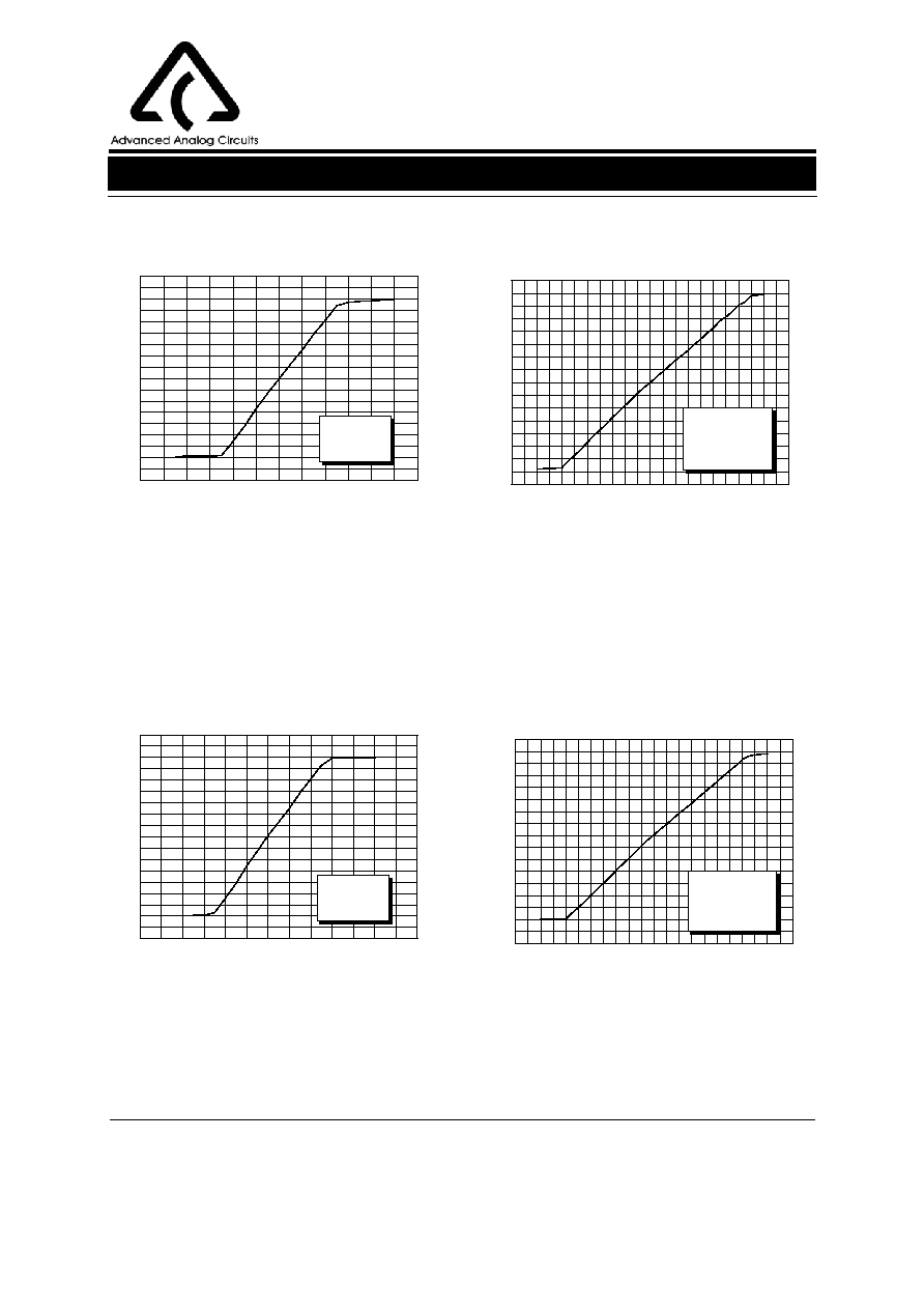
Typical Performance Characteristics (Note 2)
Figure 5. Driver I/O Characteristics (Focus)
Figure 7. Driver I/O Characteristics (Track)
-0.6
-0.4
-0.2
0.0
0.2
0.4
0.6
-4
-3
-2
-1
0
1
2
3
4
Out
p
u
t
Vol
t
age
V
O
(V
)
Input Voltage
V
IN
(V)
V
CC1
=V
CC2
=5V
V
BIAS
=1.65V
R
L
=8
+100
µ
H
-0.6
-0.4
-0.2
0.0
0.2
0.4
0.6
-4
-3
-2
-1
0
1
2
3
4
Out
p
u
t
Vol
t
age
V
O
(V
)
Input Voltage
V
IN
(V)
V
CC1
=V
CC2
=5V
V
BIAS
=1.65V
R
L
=8
+100
µ
H
Figure 6. Driver I/O Characteristics (Focus)
Figure 8. Driver I/O Characteristics (Track)
-1.0
-0.8
-0.6
-0.4
-0.2
0.0
0.2
0.4
0.6
0.8
1.0
-4
-3
-2
-1
0
1
2
3
4
O
u
tput
Volt
a
ge
V
O
(V)
Input Voltage
V
IN
(V)
V
CC1
=V
CC2
=5V
V
BIAS
=1.65V
R
L
=8
+100
µ
H
External R
IN
=18K
-1.0
-0.8
-0.6
-0.4
-0.2
0.0
0.2
0.4
0.6
0.8
1.0
-4
-3
-2
-1
0
1
2
3
4
Out
put Voltage
V
O
(V
)
Input Voltage
V
IN
(V)
V
CC1
=V
CC2
=5V
V
BIAS
=1.65V
R
L
=8
+100
µ
H
External R
IN
=20K

5-CHANNEL MOTOR DRIVER FOR DVD PLAYER AM5665
Preliminary Datasheet
9
BCD Semiconductor Manufacturing Limited
Apr. 2005 Rev. 1. 1
Figure 10. Driver I/O Characteristics (Sled)
Figure 12. Driver I/O Characteristics (Loading)
-1.0
-0.8
-0.6
-0.4
-0.2
0.0
0.2
0.4
0.6
0.8
1.0
-4
-3
-2
-1
0
1
2
3
4
O
u
t
p
ut
V
o
l
t
ag
e
V
O
(V)
Input Voltage
V
IN
(V)
V
CC1
=V
CC2
=5V
V
BIAS
=1.65V
R
L
=12
External R
IN
=10K
-2.0
-1.5
-1.0
-0.5
0.0
0.5
1.0
1.5
2.0
-4
-3
-2
-1
0
1
2
3
4
O
u
t
p
ut
V
o
l
t
ag
e
V
O
(V)
Input Voltage
V
IN
(V)
V
CC1
=V
CC2
=5V
V
BIAS
=1.65V
R
L
=12
External R
IN
=15K
Typical Performance Characteristics (Continued)
Figure 9. Driver I/O Characteristics (Sled)
-0.6
-0.4
-0.2
0.0
0.2
0.4
0.6
-4
-3
-2
-1
0
1
2
3
4
O
u
tput
V
o
lt
ag
e
V
O
(V)
Input Voltage
V
IN
(V)
V
CC1
=V
CC2
=5V
V
BIAS
=1.65V
R
L
=12
Figure 11. Driver I/O Characteristics (Loading)
-1.0
-0.8
-0.6
-0.4
-0.2
0.0
0.2
0.4
0.6
0.8
1.0
-4
-3
-2
-1
0
1
2
3
4
O
u
t
p
u
t
Vol
t
age
V
O
(V
)
Input Voltage
V
IN
(V)
V
CC1
=V
CC2
=5V
V
BIAS
=1.65V
R
L
=12
5-CHANNEL MOTOR DRIVER FOR DVD PLAYER AM5665
Preliminary Datasheet
10
Apr. 2005 Rev. 1. 1
BCD Semiconductor Manufacturing Limited
Typical Performance Characteristics (Continued)
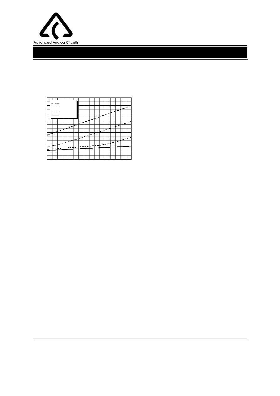
Figure 13. Tray Speed Control Characteristics
4.0
4.5
5.0
5.5
6.0
6.5
7.0
7.5
8.0
0
1
2
3
4
5
6
7
8
O
u
tput
Volt
a
ge
V
O
(V)
Input Voltage V
CC1
(V)
R
VCTL
=0
R
VCTL
=200
R
VCTL
=400
R
VCTL
=600
Note 2:
For the above figures 6, 8, 10, 12, please refer to the following "Typical Application" section.
5-CHANNEL MOTOR DRIVER FOR DVD PLAYER AM5665
Preliminary Datasheet
11
BCD Semiconductor Manufacturing Limited
Apr. 2005 Rev. 1. 1
Typical Application
Figure 14. Typical Application of AM5665 in DVD Player
21
15
16
17
18
19
20
22
23
24
25
26
27
28
8
14
13
12
11
10
9
7
6
5
4
3
2
1
STBY
0
18k
TRACK IN
330p
20K
150p
15k
SPINDLE IN
0.1
µ
0.1
µ
47
µ
5V
0
1
1
TK-
TK+
SP+
SP-
330p
20k
FOCUS IN
20k
150p
0
0.015
µ
1
1
FC-
FC+
SL+
SL-
TRAY+
TRAY-
47µ
10k
REV
10k
10k
FWD
10k
10k
SLED IN
5V
AM5665
0.1
µ
V
BIAS
5-CHANNEL MOTOR DRIVER FOR DVD PLAYER AM5665
Preliminary Datasheet
12
Apr. 2005 Rev. 1. 1
BCD Semiconductor Manufacturing Limited
Application Information
Input
Output
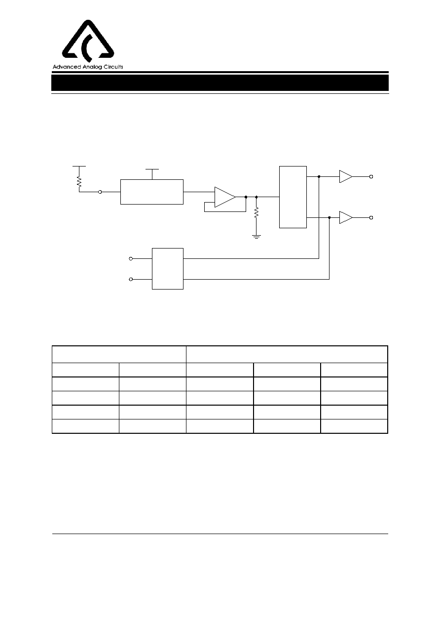
FWD
REV
VOTR+
VOTR-
Status
High
High
Low
Low
Break
High
Low
High
Low
Forward
Low
High
Low
High
Reverse
Low
Low
Open
Open
Standby
Figure 15. Tray Motor Driver Control Illustration
Tray Motor Speed Control
The amplitude of output voltage depends on VCTL (pin 21). Connect a resistor between VCTL (pin 21) and
V
CC1,
and you can obtain different output voltages for tray driver by changing the value of R
VCTL
. (See Figure 4.)
VCTL
R
VCTL
VOTR+
VOTR-
Logic
Switching
FWD
REV
Level Shift
V
CC1
V
CC1
+
-
+
-
Pre-Amp
Output Status Control Table
Tray Motor Driver
This application information is only for the Tray Motor Driver section.

5-CHANNEL MOTOR DRIVER FOR DVD PLAYER AM5665
Preliminary Datasheet
13
BCD Semiconductor Manufacturing Limited
Apr. 2005 Rev. 1. 1
Mechanical Dimensions
Unit: mm(inch)
HSOP-28
17.890(0.704)
0.204(0.008)
0
o
~
8
o
18.190(0.716)
0.360(0.014)
0.400(0.016)
1.270(0.050)
10.000(0.394)
10.650(0.419)
7.400(0.291)
7.600(0.300)
0.230(0.009)
0.470(0.019)
0.100(0.004)
0.300(0.012)
2.280(0.090)
2.630(0.104)
2.180(0.086)
2.330(0.092)
0.800(0.031)TYP
5.050(0.199)
5.250(0.207)
8F, B Zone, 900 Yi Shan Road, Shanghai 200233, PRC Tel: +86-21-6495 9539, Fax: +86-21-6485 9673
BCD Semiconductor (Taiwan) Company Limited
Room 2210, 22nd Fl, 333, Keelung Road, Sec. 1, TaiPei (110), Taiwan Tel: +886-2-2758 6828, Fax: +886-2-2758 6892
IMPORTANT NOTICE
BCD Semiconductor Manufacturing Limited reserves the right to make changes without further notice to any pro-
ducts or specifications herein. BCD Semiconductor Manufacturing Limited does not assume any responsibility for
use of any its products for any particular purpose, nor does BCD Semiconductor Manufacturing Limited assume any
liability arising out of the application or use of any its products or circuits. BCD Semiconductor Manufacturing Limi-
ted does not convey any license under its patent rights or other rights nor the rights of others.
http://www.bcdsemi.com
BCD Semiconductor Corporation
3170 De La Cruz Blvd, Suite # 105 Santa Clara, CA 95054-2411, U.S.A Tel: +1-408-988 6388, Fax: +1-408-988 6386
Shanghai SIM-BCD Semiconductor Manufacturing Co., Ltd.
800 Yi Shan Road, Shanghai 200233, PRC Tel: +86-21-6485-1491, Fax: +86-21-5450-0008
Advanced Analog Circuits (Shanghai) Corporation