
600mA LOW DROPOUT LINEAR REGULATOR AP1117M
Data Sheet
600mA LOW DROPOUT LINEAR REGULATOR AP2317
1
Sep. 2005 Rev. 1. 4
BCD Semiconductor Manufacturing Limited
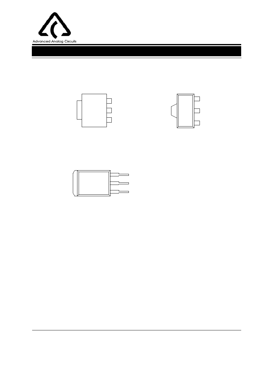
Figure 1. Package Types of AP2317
SOT-89-3
SOT-223
General Description
The AP2317 is a series of low dropout three-terminal
regulators with a dropout of 1.1V at 600mA output cur-
rent.
This product has been optimized for low voltage where
transient response and minimum input voltage are criti-
cal. The AP2317 provides current limit and thermal
shutdown. Its circuit includes a trimmed bandgap refer-
ence to assure output voltage accuracy to be within
±1%. On-chip thermal shutdown provides protection
against any combination of overload and ambient tem-
peratures that would create excessive junction tem-
peratures.
The AP2317 is available in 2.5V and 3.3V versions.
The fixed versions integrate the adjust resistors. It is
also available in an adjustable version which can set
the output voltage with two external resistors.
The AP2317 series regulators are available in the
industry standard SOT-89-3, SOT-223 and TO-263-3
(for 3.3V only) power packages.
Features
∑
Low Dropout Voltage: 1.1V at 600mA Output
Current
∑
Output Noise from 10Hz to 10KHz: 0.003%
∑
PSRR at I
OUT
=300mA and f=120Hz: 75dB
∑
Output Voltage Accuracy:
± 1%
∑
On-chip Thermal Shutdown
∑
Maximum Quiescent Current
:
I
QMAX
=5mA
∑
ESD (Human Body Model): 3.5KV
∑
Operation Junction Temperature: -40 to 125
o
C
Applications
∑
DVD/CD-ROM
∑
USB Device
∑
Add-on Card
∑
DVD Player
∑
PC Motherboard
TO-263-3
600mA LOW DROPOUT LINEAR REGULATOR AP1117M
Data Sheet
600mA LOW DROPOUT LINEAR REGULATOR AP2317
2
Sep. 2005 Rev. 1. 4
BCD Semiconductor Manufacturing Limited
Figure 2. Pin Configuration of AP2317 (Top View)
H Package
(SOT-223)
INPUT
OUTPUT
ADJ/GND
V
OUT
1
2
3
R Package
ADJ/GND
OUTPUT
INPUT
V
OUT
(SOT-89-3)
3
2
1
Pin Configuration
3
2
1
GND
OUTPUT
INPUT
S Package
(TO-263-3)

600mA LOW DROPOUT LINEAR REGULATOR AP1117M
Data Sheet
600mA LOW DROPOUT LINEAR REGULATOR AP2317
3
Sep. 2005 Rev. 1. 4
BCD Semiconductor Manufacturing Limited
Ordering Information
Circuit Type
Package
R: SOT-89-3
H: SOT-223
ADJ: Adjustable Output
2.5: Fixed Output 2.5V
3.3: Fixed Output 3.3V
E1: Lead Free
Blank: Tin Lead
AP2317 -
TR: Tape and Reel
Blank: Tube
Functional Block Diagram
Figure 3. Functional Block Diagram of AP2317
Thermal
Protection
+
-
For Adjustable Output, disconnect A1 and A2, connect B
INPUT
OUTPUT
ADJ/GND
A1
A2
B
For Fixed Output, connect A1 and A2, disconnect B
2
1
3
S: TO-263-3

600mA LOW DROPOUT LINEAR REGULATOR AP1117M
Data Sheet
600mA LOW DROPOUT LINEAR REGULATOR AP2317
4
Sep. 2005 Rev. 1. 4
BCD Semiconductor Manufacturing Limited
Recommended Operating Conditions
Note 1:
Stresses greater than those listed under "Absolute Maximum Ratings" may cause permanent damage to the
device.
These are stress ratings only, and functional operation of the device at these or any other conditions beyond those indicated
under "Recommended Operating Conditions" is not implied. Exposure to "Absolute Maximum Ratings" for extended periods
may affect device reliability.
Parameter
Symbol
Value
Unit
Input Voltage
V
IN
15
V
Operating Junction Temperature Range
T
J
150
o
C
Storage Temperature Range
T
STG
-65 to 150
o
C
Lead Temperature (Soldering, 10sec)
T
LEAD
300
o
C
ESD (Human Body Model)
ESD
3500
V
ESD (Machine Model)
ESD
400
V
Parameter
Symbol
Min
Max
Unit
Input Voltage
V
IN
12
V
Operating Junction Temperature Range
T
J
-40
125
o
C
Storage Temperature Range
T
STG
-65
150
o
C
Absolute Maximum Ratings (Note 1)
BCD Semiconductor's Pb-free products, as designated with "E1" suffix in the part number, are RoHS compliant.
Package
Temperature
Range
Part Number
Marking ID
Packing Type
Tin Lead
Lead Free
Tin Lead
Lead Free
SOT-89-3
-40 to
125
o
C
AP2317R-ADJTR
AP2317R-ADJTRE1
R27A
E27A
Tape & Reel
AP2317R-2.5TR
AP2317R-2.5TRE1
R27B
E27B
Tape & Reel
AP2317R-3.3TR
AP2317R-3.3TRE1
R27C
E27C
Tape & Reel
SOT-223
-40 to
125
o
C
AP2317H-ADJTR
AP2317H-ADJTRE1
H27A
EH27A
Tape & Reel
AP2317H-2.5TR
AP2317H-2.5TRE1
H27B
EH27B
Tape & Reel
AP2317H-3.3TR
AP2317H-3.3TRE1
H27C
EH27C
Tape & Reel
TO-263-3
-40 to
125
o
C
AP2317S-3.3
AP2317S-3.3E1
AP2317S-3.3
AP2317S-3.3E1
Tube
AP2317S-3.3TR
AP2317S-3.3TRE1
AP2317S-3.3
AP2317S-3.3E1
Tape & Reel
Ordering Information (Continued)

600mA LOW DROPOUT LINEAR REGULATOR AP1117M
Data Sheet
600mA LOW DROPOUT LINEAR REGULATOR AP2317
5
Sep. 2005 Rev. 1. 4
BCD Semiconductor Manufacturing Limited
Parameter
Symbol
Conditions
Min
Typ
Max
Unit
Reference Voltage
V
REF
AP2317-ADJ I
OUT
=10mA, V
IN
-V
OUT
=2V, T
J
=25
o
C
10mA
I
OUT
600mA, 1.4VV
IN
-V
OUT
8V
P
maximum power dissipation
1.238
1.225
1.250
1.250
1.262
1.270
V
Output Voltage
V
OUT
AP2317-2.5 I
OUT
=10mA, V
IN
=4.5V, T
J
=25
o
C
10mA
I
OUT
600mA, 3.9V V
IN
10V
2.475
2.450
2.5
2.5
2.525
2.550
V
AP2317-3.3 I
OUT
=10mA, V
IN
=5.0V, T
J
=25
o
C
10mA
I
OUT
600mA, 4.75VV
IN
10V
3.267
3.235
3.3
3.3
3.333
3.365
V
Line Regulation
V
OUT
AP2317-ADJ
I
OUT
=10mA, 1.5V
V
IN
-V
OUT
10V
0.035
0.2
%
AP2317-2.5
I
OUT
=10mA, 1.5V
V
IN
-V
OUT
10V
1
6
mV
AP2317-3.3
I
OUT
=10mA, 1.5V
V
IN
-V
OUT
10V
1
6
mV
Load Regulation
V
OUT
AP2317-ADJ
(V
IN
-V
OUT
)=2V, 10mA
I
OUT
600mA
0.2
0.4
%
AP2317-2.5
(V
IN
-V
OUT
)=2V, 10mA
I
OUT
600mA
1
10
mV
AP2317-3.3
(V
IN
-V
OUT
)=2V, 10mA
I
OUT
600mA
1
10
mV
Dropout Voltage
V
REF
=1%, I
OUT
=0.6A
1.1
1.3
V
Current Limit
I
LIMIT
(V
IN
-V
OUT
)=2V
0.75
0.9
A
Adjust Pin Current
60
120
µ
A
Adjust Pin Current
Change
1.4V
(V
IN
-V
OUT
)10, 10mAI
OUT
600mA
0.2
5
µ
A
Minimum Load Current
1.5V
(V
IN
-V
OUT
)10V (ADJ only)
1.7
5
mA
Quiescent Current
V
IN
=V
OUT
+1.25V
5
mA
Ripple Rejection
f=120Hz, C
OUT
=22
µ
F Tantalum
(V
IN
-V
OUT
)=3V, I
OUT
=300mA
60
75
dB
Temperature Stability
0.5
%
Long-Term Stability
T
A
=125
o
C, 1000hrs.
0.3
%
RMS Output Noise
T
A
=25
o
C, 10Hz
f10KHz
0.003
%
Thermal Shutdown
Junction Temperature
150
o
C
Thermal Shutdown
Hysteresis
25
o
C
Thermal Resistance
JC
SOT-89-3
37
o
C/W
SOT-223
33
TO-263-3
7
Operating Conditions: V
IN
10V,T
J
=25
o
C, unless otherwise specified. (P
maximum power dissipation)
Limits appearing in Boldface type apply over the entire junction temperature range for operation, -40
o
C to 125
o
C
Electrical Characteristics