QUAD OP AMP AND VOLTAGE REFERENCE AP4302
Data Sheet
1
Apr. 2005 Rev. 1. 1
BCD Semiconductor Manufacturing Limited
General Description
The AP4302 is a monolithic IC specifically designed
to regulate the output current and voltage levels of
switching battery chargers and power supplies.
The device contains quad Op Amps and a 2.5V exter-
nally adjusted voltage reference in a 16-pin package.
The four Op Amps feature accurate voltage and current
control. Combining a stable voltage reference with the
four Op Amps makes AP4302 ideal for use in multi-
function charger, power supply voltage monitor, signal
processing and control system.
The IC offers the power converter designer a control
solution that features increased precision with a corre-
sponding reduction in system complexity and cost.
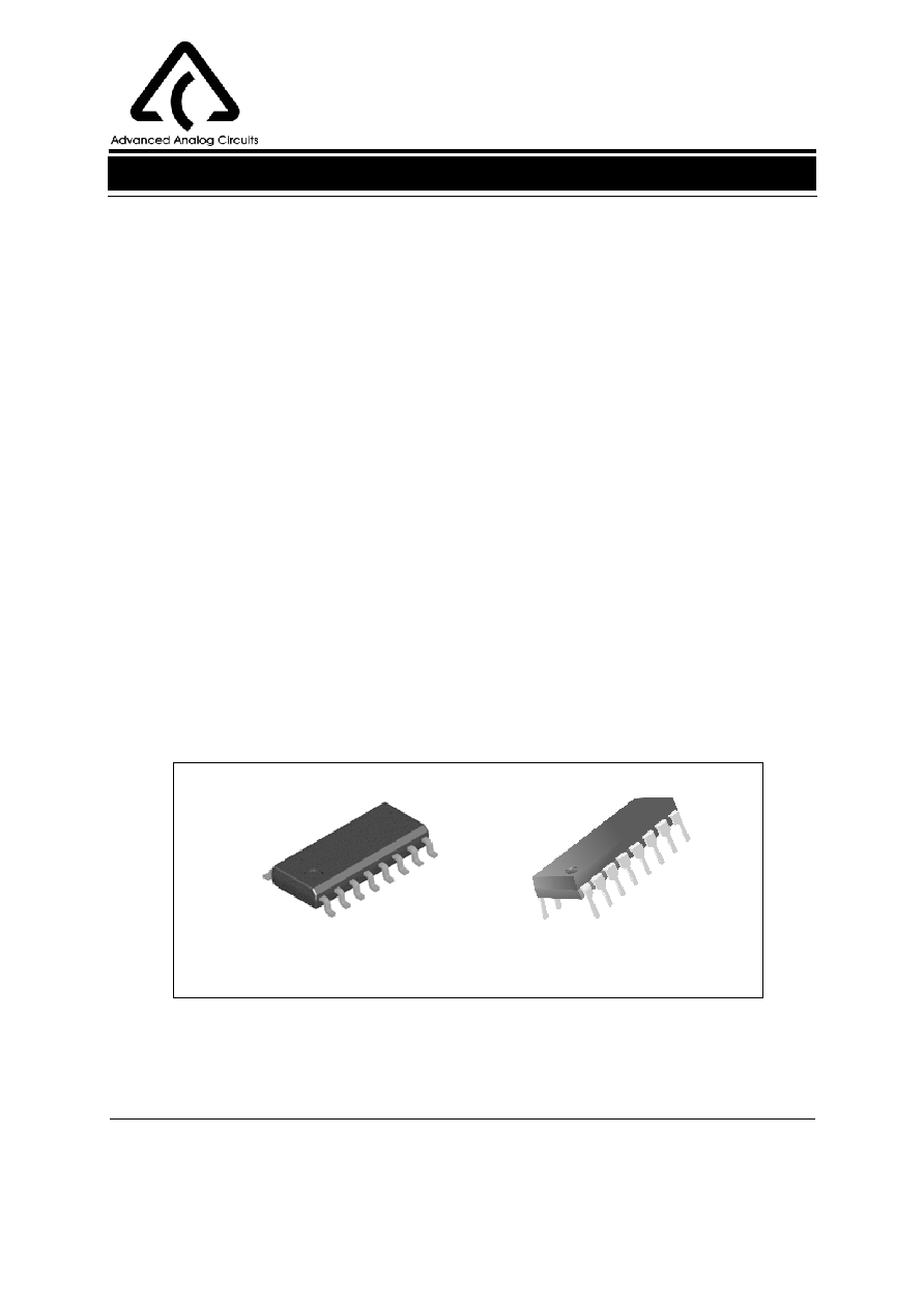
The AP4302 is available in standard packages of DIP-
16 and SOIC-16.
Features
Op Amp
∑
Input Offset Voltage: 0.5mV
∑
Supply Current: 250
µA per Op Amp at 5.0V Sup-
ply Voltage
∑
Unity Gain Bandwidth: 1MHz
∑
Output Voltage Swing: 0 to (V
CC
- 1.5)V
∑
Power Supply Range: 3 to 18V
Voltage Reference
∑
Reference Voltage Tolerance: 0.5%, 1%
∑
Sink Current Capability from 0.1 to 80mA
∑
Output Dynamic Impedance: 0.2
∑
Externally Adjusted Voltage Reference: 2.5V
Applications
∑
Battery Charger
∑
Switching Power Supply
Figure 1. Package Types of AP4302
SOIC-16
DIP-16
QUAD OP AMP AND VOLTAGE REFERENCE AP4302
Data Sheet
2
Apr. 2005 Rev. 1. 1
BCD Semiconductor Manufacturing Limited
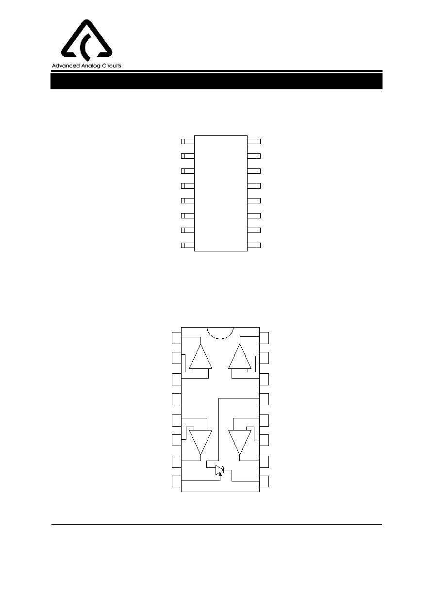
Functional Block Diagram
Pin Configuration
Figure 2. Pin configuration of AP4302
INPUT 1-
INPUT 1+
V
CC
OUTPUT 4
INPUT 4-
INPUT 4+
GND
Top View
OUTPUT 1
INPUT 2+
INPUT 2-
OUTPUT 2
V
REF
INPUT 3+
INPUT 3-
OUTPUT 3
CATHODE
1
2
3
4
5
6
7
8
16
15
14
13
12
11
10
9
Figure 3. Functional Block Diagram of AP4302
-
+
-
-
-
+
+
+
OUTPUT 4
INPUT 4-
INPUT 4+
GND
CATHODE
OUTPUT 3
INPUT 3-
INPUT 3+
V
REF
OUTPUT 2
INPUT 2-
INPUT 2+
V
CC
INPUT 1+
INPUT 1-
OUTPUT 1
1
2
3
4
5
6
7
8
16
15
14
13
12
11
10
9
(SOIC-16/DIP-16)
M Package/P Package
QUAD OP AMP AND VOLTAGE REFERENCE AP4302
Data Sheet
3
Apr. 2005 Rev. 1. 1
BCD Semiconductor Manufacturing Limited
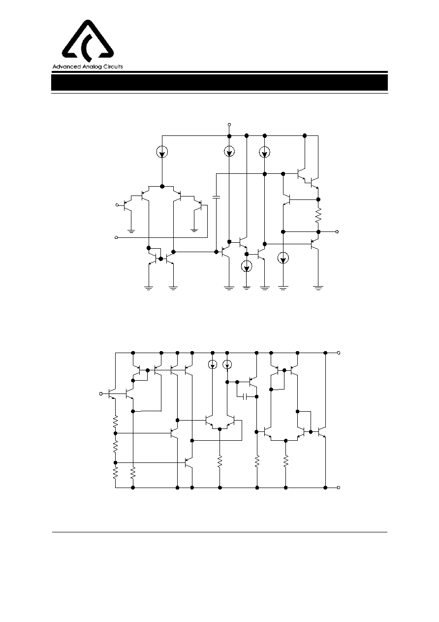
Figure 5. Voltage Reference Functional Block Diagram
Functional Block Diagram (Continued)
Figure 4. Op Amp Functional Block Diagram
(Each Amplifier)
Q2
Q4
Q3
Q1
Q8
Q9
6
µ
A
4
µ
A
Q10
Q11
50uA
Q5
Q6
Q13
Rsc
Cc
100
µ
A
Q7
INPUT-
INPUT+
OUTPUT
Q12
V
CC
CATHODE
GND
V
REF
20
µ
A
20
µ
A
QUAD OP AMP AND VOLTAGE REFERENCE AP4302
Data Sheet
4
Apr. 2005 Rev. 1. 1
BCD Semiconductor Manufacturing Limited
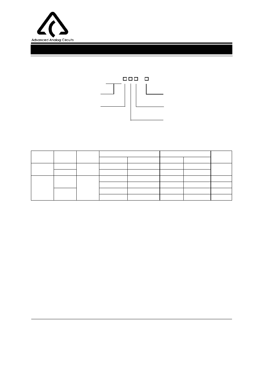
Package
Voltage Tol-
erance
Tempera-
ture Range
Part Number
Marking ID
Packing
Type
Tin Lead
Lead Free
Tin Lead
Lead Free
DIP-16
0.5%
-40 to 85
o
C AP4302AP
AP4302AP-E1
AP4302AP
AP4302AP-E1
Tube
1%
AP4302BP
AP4302BP-E1
AP4302BP
AP4302BP-E1
SOIC-16
0.5%
-40 to 85
o
C
AP4302AM
AP4302AM-E1
AP4302AM
AP4302AM-E1
Tube
AP4302AMTR
AP4302AMTR-E1
AP4302AM
AP4302AM-E1
Tape & Reel
1%
AP4302BM
AP4302BM-E1
AP4302BM
AP4302BM-E1
Tube
AP4302BMTR
AP4302BMTR-E1
AP4302BM
AP4302BM-E1
Tape & Reel
BCD Semiconductor's Pb-free products, as designated with "E1" suffix in the part number, are RoHS compliant.
Circuit Type
Voltage Tolerance
A: 0.5%
B: 1%
Package
P: DIP-16
M: SOIC-16
AP4302 -
E1: Lead-free
Blank: Tin Lead
TR: Tape and Reel
Blank: Tube
Ordering Information
QUAD OP AMP AND VOLTAGE REFERENCE AP4302
Data Sheet
5
Apr. 2005 Rev. 1. 1
BCD Semiconductor Manufacturing Limited
Parameter
Min
Max
Unit
Supply Voltage
3
18
V
Ambient Temperature
-40
85
o
C
Recommended Operating Conditions
Note 1: Stresses greater than those listed under "Absolute Maximum Ratings" may cause permanent damage to the
device. These are stress ratings only, and functional operation of the device at these or any other conditions beyond
those indicated under "Recommended Operating Conditions" is not implied. Exposure to "Absolute Maximum
Ratings " for extended periods may affect device reliability.
Parameter
Symbol
Value
Unit
Power Supply Voltage (V
CC
to GND)
V
CC
20
V
Input Voltage Range
V
IN
-0.3 to V
CC
+ 0.3
V
Op Amp Input Differential Voltage
V
ID
20
V
Voltage Reference Cathode Current
I
K
100
mA
Power Dissipation
DIP-16
P
D
1000
mW
SOIC-16
1000
Storage Temperature Range
T
STG
-65 to 150
o
C
ESD Protection Voltage (Machine Model)
>200
V
Absolute Maximum Ratings (Note 1)

QUAD OP AMP AND VOLTAGE REFERENCE AP4302
Data Sheet
6
Apr. 2005 Rev. 1. 1
BCD Semiconductor Manufacturing Limited
Operating Conditions: V
CC
=
+
5V, T
A
= 25
o
C unless otherwise specified.
Electrical Characteristics
Parameter
Conditions
Min
Typ
Max
Unit
Total Supply Current, Excluding
Current in Voltage Reference
V
CC
= 5V, no load, -40
o
C
T
A
85
o
C
1.0
1.6
mA
V
CC
= 18V, no load, -40
o
C
T
A
85
o
C
1.2
2.4
Voltage Reference Section
Reference Voltage
I
KA
= 10mA
T
A
= 25
o
C
0.5% tolerance
2.487
2.500
2.513
V
1% tolerance
2.475
2.525
Reference Voltage Deviation over
Full Temperature Range
I
KA
= 10mA, T
A
= -40 to 85
o
C
5
24
mV
Minimum Cathode Current
for Regulation
0.1
0.2
mA
Ratio of Change in V
REF
to that of
Cathode Voltage
I
KA
= 10mA
V
REF
to 10V
1.0
2.7
mV/V
10V to 18V
0.5
2.0
Reference Current
I
KA
= 10mA, R1 = 10K, R2 =
0.7
4
µA
The Deviation of Reference Current
over Temperature
V
KA
= V
REF
, I
KA
= 10mA,
T
A
= -40 to 85
o
C
0.4
1.2
µA
Off-State Cathode Current
V
REF
= 0, V
KA
= 18V
0.05
1.0
µA
Dynamic Impedance
I
KA
= 1.0 to 80mA, f<1kHz
0.2
0.5
QUAD OP AMP AND VOLTAGE REFERENCE AP4302
Data Sheet
7
Apr. 2005 Rev. 1. 1
BCD Semiconductor Manufacturing Limited
Electrical Characteristics (Continued)
Operating Conditions: V
CC
=
+
5V, T
A
= 25
o
C unless otherwise specified.
Parameter
Conditions
Min
Typ
Max
Unit
Op Amp Section (per Op Amp)
(V
CC
= 5V, V
O
= 1.4V, T
A
= 25
o
C, unless otherwise noted)
Input Offset Voltage
T
A
= 25
o
C
0.5
3
mV
T
A
= -40 to 85
o
C
5
Input Offset Voltage Temperature
Drift
T
A
= -40 to 85
o
C
7
µV/
o
C
Input Offset Current
T
A
= 25
o
C
2
30
nA
Input Bias Current
T
A
= 25
o
C
20
150
nA
Input Voltage Range
V
CC
= 0 to 18V
0
V
CC
-
1.5
V
Common Mode Rejection Ratio
T
A
= 25
o
C, V
CM
= 0 to 3.5V
70
85
dB
Large Signal Voltage Gain
V
CC
= 15V, R
L
= 2k
, V
O
= 1.4 to 11.4V
85
100
dB
Power Supply Rejection Ratio
V
CC
= 5 to 18V
70
90
dB
Output Current
Source
V
CC
= 15V, V
ID
= 1V, V
O
= 2V
20
40
mA
Sink V
CC
= 15V, V
ID
= -1V, V
O
= 2V
10
20
mA
Output Voltage Swing (High)
V
CC
= 18, R
L
= 10k
, V
ID
= 1V
16
16.5
V
Output Voltage Swing (Low)
V
CC
= 18, R
L
= 10k
, V
ID
= -1V
17
100
mV
Slew Rate
V
CC
= 18V, R
L
= 2k
, A
V
= 1,
V
IN
= 0.5 to 2V, C
L
= 100pF
0.3
0.5
V/
µ s
Gain Bandwidth Product
V
CC
= 18V, R
L
= 2k
, C
L
= 100pF,
V
IN
= 10mV, f=100kHz
0.7
1
MHz
QUAD OP AMP AND VOLTAGE REFERENCE AP4302
Data Sheet
8
Apr. 2005 Rev. 1. 1
BCD Semiconductor Manufacturing Limited
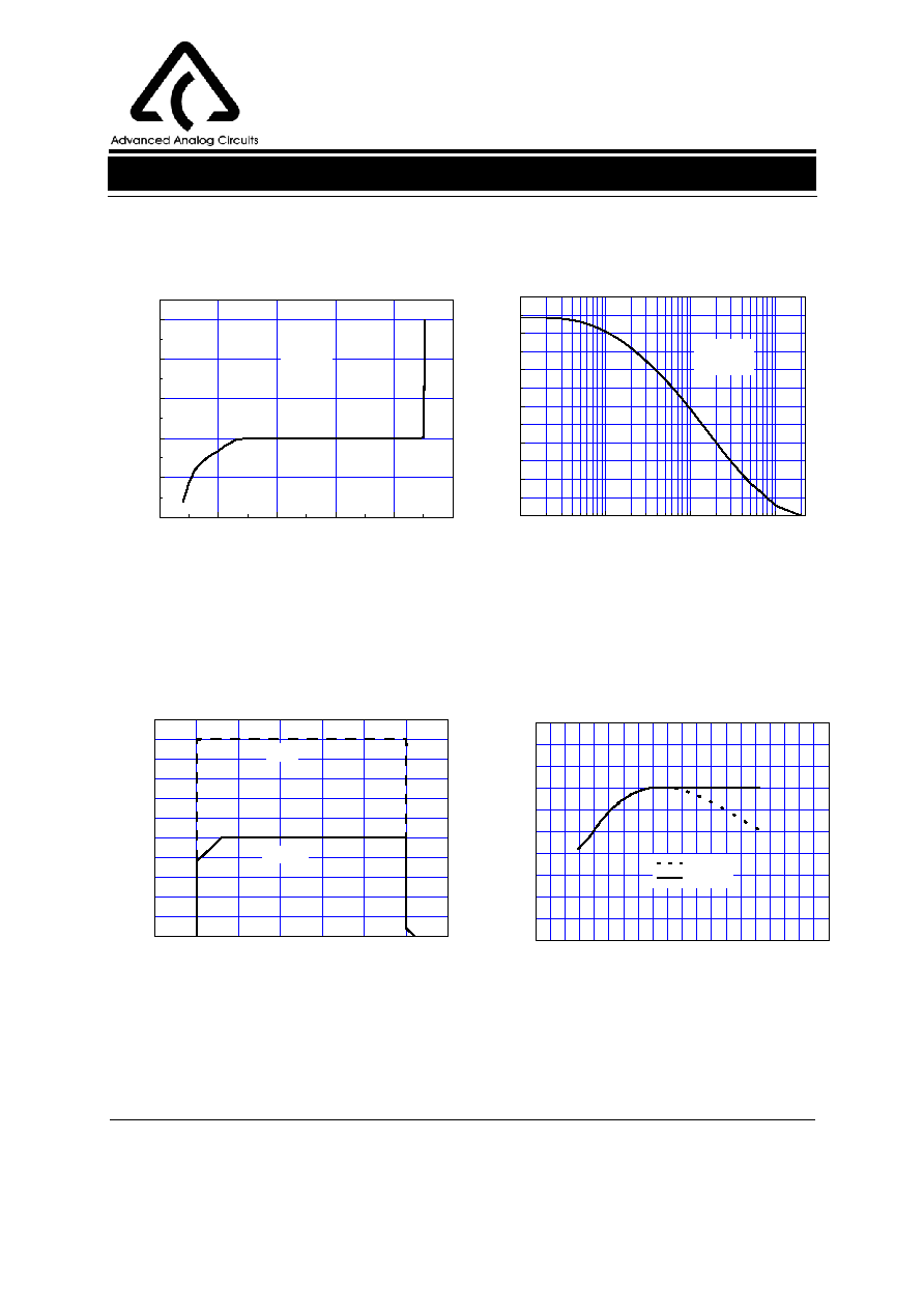
Typical Performance Characteristics
Figure 6. Cathode Current vs. Cathode Voltage
-2
-1
0
1
2
3
-100
-50
0
50
100
150
Cat
h
ode Current
(m
A
)
Cathode Voltage (V)
V
KA
=V
REF
T
A
=25
0
C
1K
10K
100K
1000K
0
10
20
30
40
50
60
0
10
20
30
40
50
60
T
A
= 25
o
C
I
KA
= 10mA
Av
(
d
B
)
Small Signal Frequency
Figure 7. Voltage Reference Small Signal Voltage Gain
vs. Frequency
Figure 8. Pulse Response of Input and Output Voltage
Figure 9. Op Amp Voltage Gain
0
2
4
6
0
1
2
3
4
5
Input
In
put and O
u
tp
ut V
o
lt
age (V
)
Time (
µ
S)
Output
0
2
4
6
8
10
12
14
16
18
20
60
70
80
90
100
110
V
o
lt
age Gain
(d
B)
Supply Voltage (V)
R
L
=2K
R
L
=20K
QUAD OP AMP AND VOLTAGE REFERENCE AP4302
Data Sheet
9
Apr. 2005 Rev. 1. 1
BCD Semiconductor Manufacturing Limited
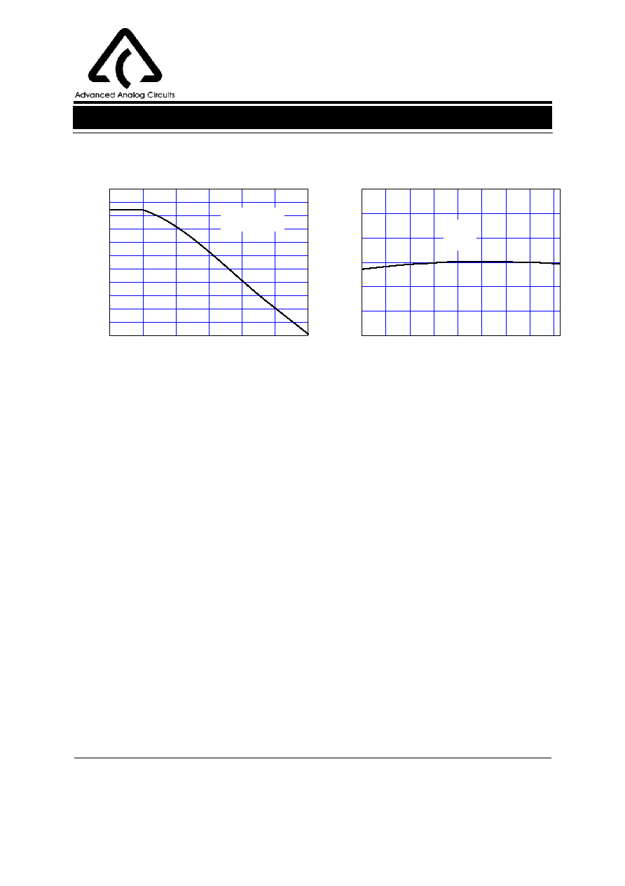
Typical Performance Characteristics (Continued)
Figure 10. Op Amp Open Loop Frequency Response
-40
-20
0
20
40
60
80
100
120
0
5
10
15
20
25
30
Ambient Temperature (
o
C)
I
nput
B
i
as
Current
(nA
)
V
CC
=15V
Figure 11. Op Amp Input Current
1HZ
10HZ
100HZ
1kHZ
10kHZ
100kHZ
1MHZ
0
10
20
30
40
50
60
70
80
90
100
110
V
o
lta
ge G
a
in
(
d
B
)
Frequency (Hz)
T
A
: -40
o
C to 85
o
C
QUAD OP AMP AND VOLTAGE REFERENCE AP4302
Data Sheet
10
Apr. 2005 Rev. 1. 1
BCD Semiconductor Manufacturing Limited
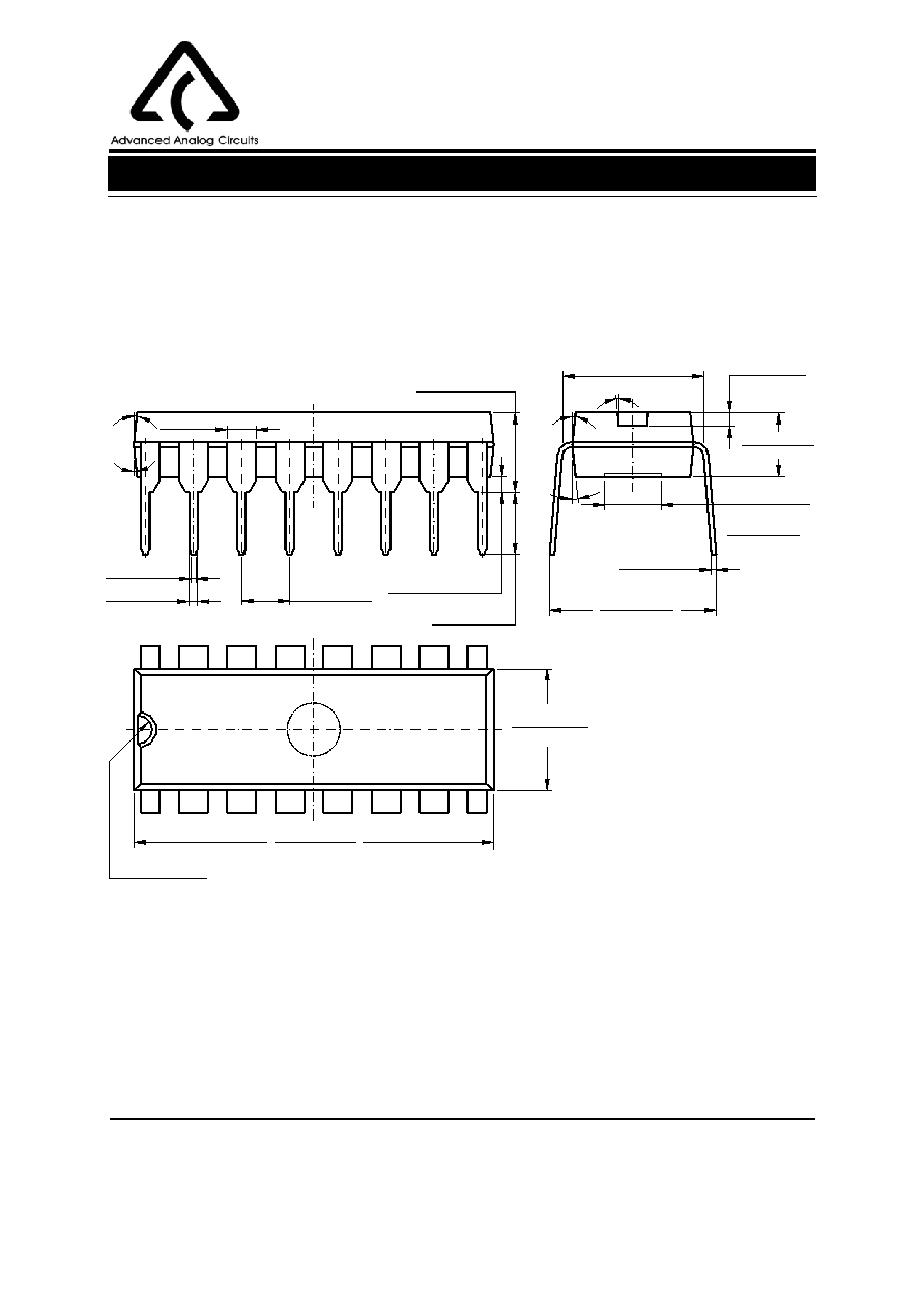
Mechanical Dimensions
DIP-16
Unit: mm(inch)
18.800(0.740)
0.254(0.010)
2.540(0.100)
6
∞
4
∞
1.524(0.060)TYP
5
∞
4
∞
6
∞
3.000(0.118)
Depth
0.050(0.002)
0.150(0.006)
0.700(0.028)
19.200(0.756)
R0.750(0.030)
6.200(0.244)
3.000(0.118)
3.600(0.142)
3.710(0.146)
4.310(0.170)
0.510(0.020)MIN
0.360(0.014)
0.560(0.022)
6.600(0.260)
8.200(0.323)
9.400(0.370)
0.204(0.008)
0.360(0.014)
3.200(0.126)
3.600(0.142)
7.620(0.300)TYP
TYP
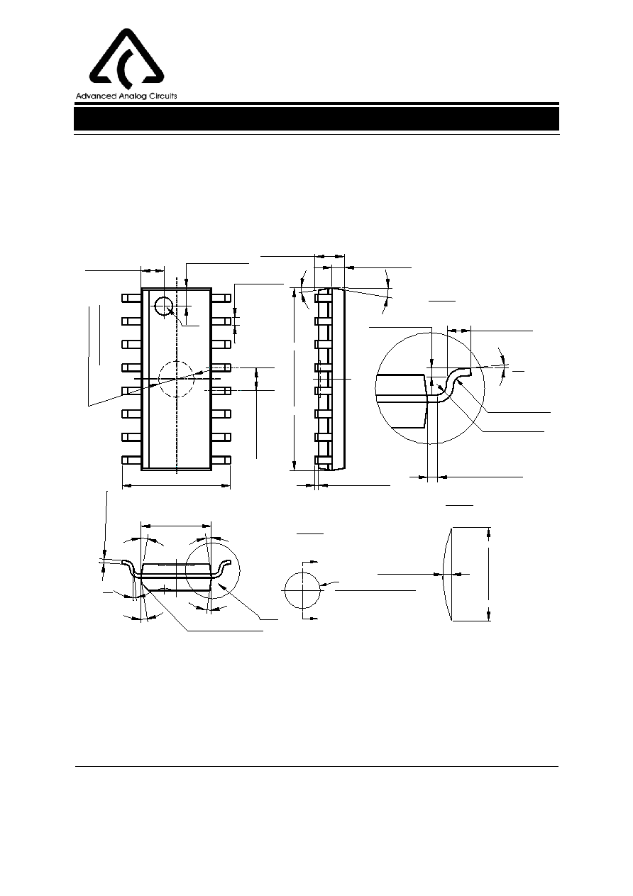
QUAD OP AMP AND VOLTAGE REFERENCE AP4302
Data Sheet
11
Apr. 2005 Rev. 1. 1
BCD Semiconductor Manufacturing Limited
SOIC-16
Unit: mm(inch)
7
∞
1
0
.
0
0
0
(
0
.
3
9
4
)
6.040(0.238)
0.406(0.016)
20:1
A
1.650(0.065)
0.700(0.028)
7
∞
1
∞
5
∞
B
C
1
.
0
0
0
(
0
.
0
3
9
)
S 1.000(0.039)
0.200(0.008)
20:1
B
C
50:1
C-C
0.250(0.010)
0.200(0.008)MIN
0.500(0.020)
0.600(0.024)
0.250(0.010)
D
e
p
t
h
0.
06
0(
0.
00
2)
0.
10
0(
0.
00
4)
2.
0
0
0
(
0.
07
9)
1.300(0.051)
1.000(0.039)
1
.
27
0(0
.
05
0)
Depth 0.200(0.008)
0.250(0.010)
0.150(0.006)
R0.200(0.008)
R0.200(0.008)
0
.
20
3(
0.
0
08
)
A
3.940(0.155)
3
∞
8
∞
9.5
∞
8
∞
8
∞
7
∞
0.400(0.016)
◊
45
∞
Mechanical Dimensions (Continued)

8F, B Zone, 900 Yi Shan Road, Shanghai 200233, PRC Tel: +86-21-6495 9539, Fax: +86-21-6485 9673
BCD Semiconductor (Taiwan) Company Limited
Room 2210, 22nd Fl, 333, Keelung Road, Sec. 1, TaiPei (110), Taiwan Tel: +886-2-2758 6828, Fax: +886-2-2758 6892
IMPORTANT NOTICE
BCD Semiconductor Manufacturing Limited reserves the right to make changes without further notice to any pro-
ducts or specifications herein. BCD Semiconductor Manufacturing Limited does not assume any responsibility for
use of any its products for any particular purpose, nor does BCD Semiconductor Manufacturing Limited assume any
liability arising out of the application or use of any its products or circuits. BCD Semiconductor Manufacturing Limi-
ted does not convey any license under its patent rights or other rights nor the rights of others.
http://www.bcdsemi.com
BCD Semiconductor Corporation
3170 De La Cruz Blvd, Suite # 105 Santa Clara, CA 95054-2411, U.S.A Tel: +1-408-988 6388, Fax: +1-408-988 6386
Shanghai SIM-BCD Semiconductor Manufacturing Co., Ltd.
800 Yi Shan Road, Shanghai 200233, PRC Tel: +86-21-6485-1491, Fax: +86-21-5450-0008
Advanced Analog Circuits (Shanghai) Corporation