 | –≠–ª–µ–∫—Ç—Ä–æ–Ω–Ω—ã–π –∫–æ–º–ø–æ–Ω–µ–Ω—Ç: AZ317 | –°–∫–∞—á–∞—Ç—å:  PDF PDF  ZIP ZIP |
3-TERMINAL 1A ADJUSTABLE VOLTAGE REGULATOR AZ317
Data Sheet
1
Apr. 2005 Rev. 1. 2
BCD Semiconductor Manufacturing Limited
General Description
The AZ317 is an adjustable three-terminal positive
voltage regulator with a very low dropout of 1.2V at
1A output current. Using 2 external resistors, the
AZ317 can provide an adjustable output voltage down
to 1.25V.
The AZ317 includes a circuit of trimmed bandgap ref-
erence to assure output voltage accuracy to be within
1%. It also provides current limiting and thermal shut-
down. The current limit is trimmed to ensure specified
output current and controlled short-circuit current. The
On-chip thermal limiting provides protection against
any combination of overload and ambient temperature
that would create excessive junction temperature.
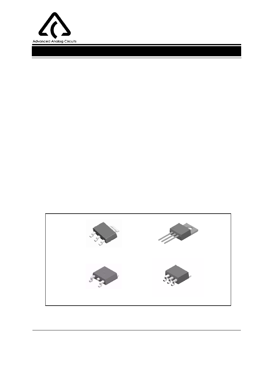
The AZ317 is available in the standard SOT-223, TO-
220, TO-252 and TO-263 power packages.
Features
∑
Typical 1% Output Voltage Tolerance
∑
Typical 0.01%/V Line Regulation
∑
Typical 0.2% Load Regulation
∑
Very Low Dropout Voltage: 1.2V at 1A Output
Current
∑
Trimmed Current Limit
∑
On-chip Thermal Protection
∑
Operation Junction Temperature: 0 to 125
o
C
Applications
∑
PC Motherboard
∑
LCD Monitor
∑
Graphic Card
∑
DVD Player
∑
Network Interface Card/Switch
∑
Telecom Equipment
∑
Printer and other Peripheral Equipment
Figure 1. Package Types of AZ317
SOT-223
TO-220
TO-252
TO-263

3-TERMINAL 1A ADJUSTABLE VOLTAGE REGULATOR AZ317
Data Sheet
2
Apr. 2005 Rev. 1. 2
BCD Semiconductor Manufacturing Limited
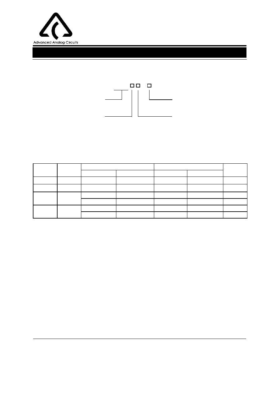
H Package
(SOT-223)
T Package
(TO-220)
(TO-252)
D Package
Pin Configuration
Functional Block Diagram
Figure 3. Functional Block Diagram of AZ317
INPUT
OUTPUT
ADJ
V
OUT
Figure 2. Pin Configuration of AZ317 (Top View)
1
2
3
INPUT
OUTPUT
ADJ
V
OUT
1
2
3
INPUT
OUTPUT
ADJ
INPUT
OUTPUT
ADJ
V
OUT
1
2
3
Thermal
Shutdown
+
+
_
Current
Limiter
S Package
(TO-263)
INPUT
OUTPUT
ADJ
1
2
3
1
2
3
3-TERMINAL 1A ADJUSTABLE VOLTAGE REGULATOR AZ317
Data Sheet
3
Apr. 2005 Rev. 1. 2
BCD Semiconductor Manufacturing Limited
Package
Tempera-
ture Range
Part Number
Marking ID
Packing
Type
Tin Lead
Lead Free
Tin Lead
Lead Free
SOT-223
0 to
125
o
C
AZ317HTR
AZ317HTR-E1
317H
EH31A
Tape & Reel
TO-220
0 to
125
o
C
AZ317T
AZ317T-E1
AZ317T
AZ317T-E1
Tube
TO-252
0 to
125
o
C
AZ317D
AZ317D-E1
AZ317D
AZ317D-E1
Tube
AZ317DTR
AZ317DTR-E1
AZ317D
AZ317D-E1
Tape & Reel
TO-263
0 to
125
o
C
AZ317S
AZ317S-E1
AZ317S
AZ317S-E1
Tube
AZ317STR
AZ317STR-E1
AZ317S
AZ317S-E1
Tape & Reel
Circuit Type
Package
H: SOT-223
E1: Lead Free
Blank: Tin Lead
AZ317 -
TR: Tape and Reel
Blank: Tube
T: TO-220
D: TO-252
S: TO-263
BCD Semiconductor's Pb-free products, as designated with "E1" suffix in the part number, are RoHS compliant.
Ordering Information

3-TERMINAL 1A ADJUSTABLE VOLTAGE REGULATOR AZ317
Data Sheet
4
Apr. 2005 Rev. 1. 2
BCD Semiconductor Manufacturing Limited
Parameter
Symbol
Min
Max
Unit
Input Voltage
V
IN
V
OUT
+2
15
V
Operating Junction Temperature Range
T
J
0
125
o
C
Recommended Operating Conditions
Note1: Stresses greater than those listed under "Absolute Maximum Ratings" may cause permanent damage to the
device. These are stress ratings only, and functional operation of the device at these or any other conditions beyond
those indicated under "Recommended Operating Conditions" is not implied. Exposure to "Absolute Maximum
Ratings" for extended periods may affect device reliability.
Parameter
Symbol
Min
Max
Unit
Input Voltage
V
IN
20
V
Maximum Junction Temperature
T
J
150
o
C
Storage Temperature
T
S
-65
150
o
C
Lead Temperature (Soldering, 10sec)
T
LEAD
300
o
C
ESD (Human Body Model)
ESD
4000
V
Absolute Maximum Ratings (Note 1)

3-TERMINAL 1A ADJUSTABLE VOLTAGE REGULATOR AZ317
Data Sheet
5
Apr. 2005 Rev. 1. 2
BCD Semiconductor Manufacturing Limited
Parameter
Symbol Conditions
Min
Typ
Max
Unit
Reference Voltage
V
REF
10mA
I
OUT
1A,
3V
(V
IN
-V
OUT
)
10V
1.20
1.25
1.30
V
Line Regulation
S
V
I
OUT
20mA, 3VV
IN
-V
OUT
10V
0.01
0.04
%/V
Load Regulation
Si
V
IN
-V
OUT
= 2V, 10mA
I
OUT
1A
0.2
0.4
%
Thermal Regulation
20ms Pulse
0.04
0.07
%/W
Dropout Voltage
V
I
OUT
= 1A
1.2
1.3
V
Current Limit
I
LIMIT
(V
IN
-V
OUT
) = 2V
1.2
1.5
1.8
A
Adjust Pin Current
50
100
µA
Adjust Pin Current Change
1.4V
(V
IN
-V
OUT
)
10V,
10mA
I
OUT
1A
0.2
5
µA
Minimum Load Current
3V
(V
IN
-V
OUT
)
15V
3.5
10
mA
Ripple Rejection
f =120Hz, C
OUT
=1
µF Tantalum,
(V
IN
-V
OUT
) = 3V, I
OUT
=1A
60
75
dB
Temperature Stability
1
%
Long -Term Stability
T
A
=125
o
C, 1000hrs
0.3
%
RMS Output Noise (% of V
OUT
)
T
A
=25
o
C, 10Hz
f 10kHz
0.003
%
Thermal Resistance,
Junction to Case
SOT-223
TO-252
TO-220
TO-263
15
10
4.5
4
o
C/W
Thermal Shutdown
Junction Temperature
150
o
C
Thermal Shutdown Hysteresis
25
o
C
(Typicals and limits apply for T
J
=25
o
C,
P
Maximum Power Dissipation
unless otherwise specified.)(Note 2)
Note 2: Maximum Power Dissipation is Package Type and Case Temperature dependent. Please see Figure 12.
Electrical Characteristics

3-TERMINAL 1A ADJUSTABLE VOLTAGE REGULATOR AZ317
Data Sheet
6
Apr. 2005 Rev. 1. 2
BCD Semiconductor Manufacturing Limited
Typical Performance Characteristics
Figure 5. Dropout Voltage vs. Output Current
Figure 6. Load Regulation vs. Temperature
Figure 7. Reference Voltage vs. Temperature
Figure 8. Output Voltage vs. Temperature
0
25
50
75
100
125
3.10
3.15
3.20
3.25
3.30
3.35
3.40
V
OUT
=3.3V
I
OUT
=30mA
O
u
t
p
u
t
V
o
lt
ag
e
(
V
)
Ambient Temperature (
o
C)
0.2
0.4
0.6
0.8
1.0
0.5
0.6
0.7
0.8
0.9
1.0
1.1
1.2
T
A
=120
o
C
T
A
=25
o
C
T
A
=0
o
C
D
r
opou
t V
o
ltag
e
(
V
)
Output Current (A)
0
20
40
60
80
100
120
-0.2
0.0
0.2
0.4
0.6
0.8
V
OUT
=3.3V
Out
p
ut V
o
lt
age
Dev
i
at
i
o
n (%)
Ambient Temperature (
o
C)
0
25
50
75
100
125
1.210
1.215
1.220
1.225
1.230
1.235
1.240
1.245
1.250
1.255
1.260
V
OUT
=3.3V
I
OUT
=30mA
Re
f
e
re
nc
e
V
o
lt
ag
e (
V
)
Ambient Temparature (
o
C)

3-TERMINAL 1A ADJUSTABLE VOLTAGE REGULATOR AZ317
Data Sheet
7
Apr. 2005 Rev. 1. 2
BCD Semiconductor Manufacturing Limited
Figure 9. Minimum Load Current vs. Temperature
Figure 11. Short-Circuit Current vs. Temperature
Figure 12. Maximum Power Dissipation
Typical Performance Characteristics (Continued)
25
50
75
100
125
0.0
2.5
5.0
7.5
10.0
SOT- 223
Po
w
e
r
(W)
Case Temperature (
o
C)
Figure 10.
Adjust Pin Current vs. Temperature
0
25
50
75
100
125
1.00
1.25
1.50
1.75
2.00
S
hor
t-
Circ
uit
C
u
rr
ent
(
A
)
Junction Temperature (
o
C)
0
25
50
75
100
125
0
1
2
3
4
5
V
OUT
=3.3V
Mi
ni
mum Lo
ad
Cu
rren
t
(mA)
Ambient Temperature (
o
C)
0
25
50
75
100
125
0
10
20
30
40
50
60
70
80
90
100
V
OUT
=3.3V
I
OUT
=30mA
Adju
st
Pin Cu
rr
e
n
t
(
µ
A)
Ambient Temperature(
o
C)
3-TERMINAL 1A ADJUSTABLE VOLTAGE REGULATOR AZ317
Data Sheet
8
Apr. 2005 Rev. 1. 2
BCD Semiconductor Manufacturing Limited
Typical Performance Characteristics (Continued)
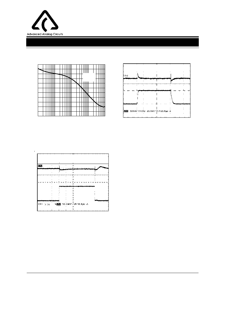
Figure 13. Ripple Rejection vs. Frequency
Figure 14. Line Transient Response
Figure 15. Load Transient Response
10
100
1k
10k
100k
20
30
40
50
60
70
V
IN
=8.3V
V
OUT
=3.3V
R
i
pp
le
R
e
je
c
t
io
n
(
d
B
)
Frequency (Hz)
Line_transient_response
V
IN
=4.8V, V
OUT
=3.33V, C
IN
=1
µ,C
OUT
=10
µ (TAN)
V
OUT
V
IN
=5.8V
V
IN
=4.8V
V
IN
=4.8V, V
OUT
=3.33V, C
IN
=C
OUT
=10
µ (TAN)
preload=0.1A
Line_transient_response
V
OUT
I
OUT
=0.5A
I
OUT
=0.1A
3-TERMINAL 1A ADJUSTABLE VOLTAGE REGULATOR AZ317
Data Sheet
9
Apr. 2005 Rev. 1. 2
BCD Semiconductor Manufacturing Limited
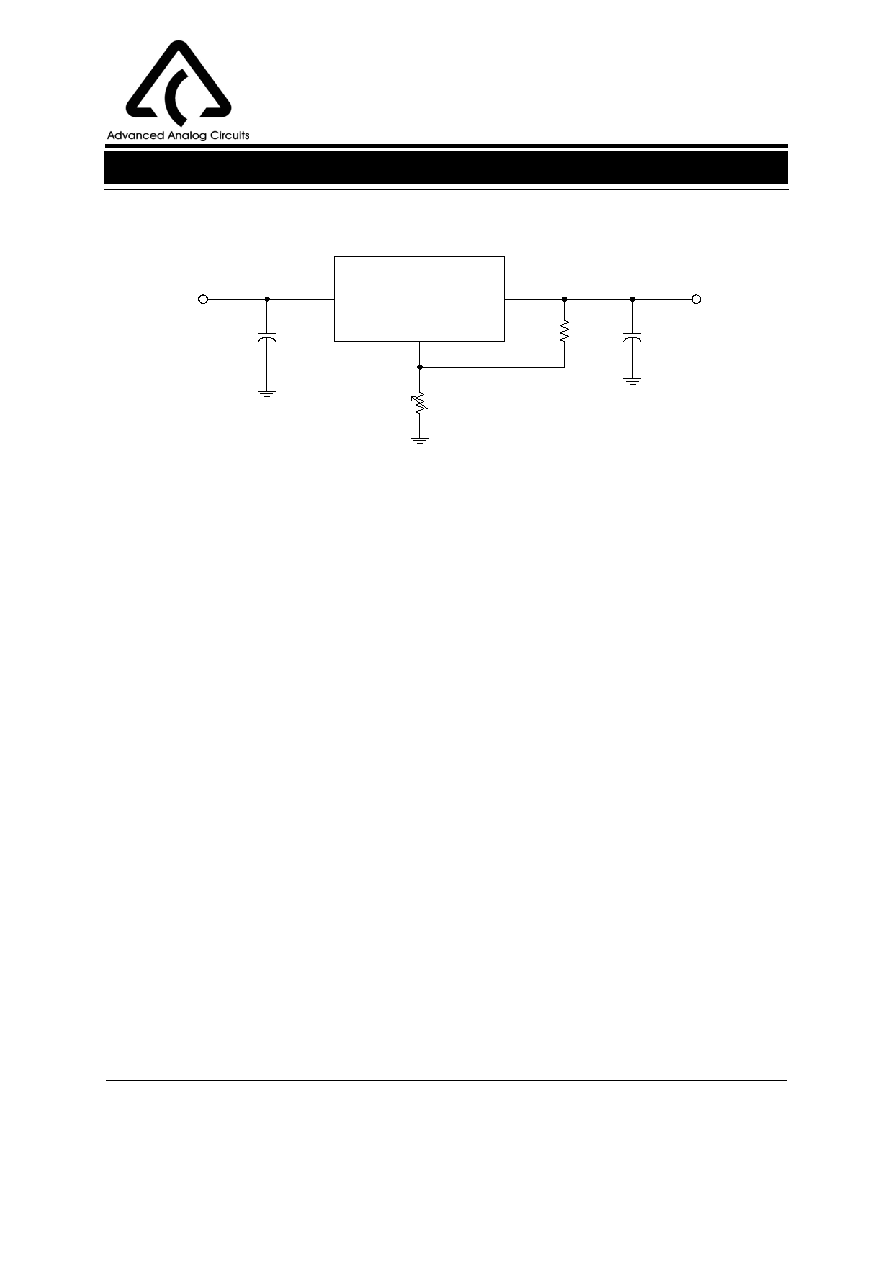
Typical Application
Figure 4. Typical Application of AZ317
V
OUT
= V
REF
x (1+R2/R1) + I
ADJ
x R2
Since I
ADJ
is controlled to less than 100
µ
A, the error associated with this term is negligible
in most applications.
* = C
IN
is required if the regulator is located near power supply filter.
**= C
O
is needed for stability and it improves transient response.
AZ317
OUTPUT
INPUT
ADJ
+
+
*
C
IN
0.1
µ
F
**
C
O
1.0
µ
F
V
IN
V
OUT
R1
240
R2
3-TERMINAL 1A ADJUSTABLE VOLTAGE REGULATOR AZ317
Data Sheet
10
Apr. 2005 Rev. 1. 2
BCD Semiconductor Manufacturing Limited
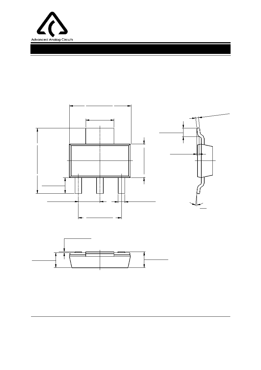
Mechanical Dimensions
SOT-223
Unit: mm(inch)
3.
3
0
0(0.
13
0
)
3.
7
0
0(0.
14
6
)
6.70
0(
0.
26
4)
7
.
30
0(0
.
2
8
7)
2.900(0.114)
3.100(0.122)
0.610(0.024)
0.810(0.032)
2.300(0.091)
TYP
6.300(0.248)
6.700(0.264)
1.750(0.069)
TYP
4.500(0.177)
4.700(0.185)
0.020(0.001)
0.100(0.004)
1.520(0.060)
1.800(0.071)
1.500(0.059)
1.700(0.067)
0.250(0.010)
0.350(0.014)
0.250(0.010)
0
∞
10
∞
0.900(0.035)
MIN

3-TERMINAL 1A ADJUSTABLE VOLTAGE REGULATOR AZ317
Data Sheet
11
Apr. 2005 Rev. 1. 2
BCD Semiconductor Manufacturing Limited
Mechanical Dimensions (Continued)
TO-220
Unit: mm(inch)
3.560(0.140)
1
4
.
2
3
0
(
0
.
5
6
0
)
1.160(0.046)
0.813(0.032)
8.763(0.345)
2.540(0.100)
0.356(0.014)
2.080(0.082)
3
∞
7
∞
3.560(0.140)
7
∞
9.660(0.380)
0.550(0.022)
60
∞
0.381(0.015)
2.580(0.102)
60
∞
8
.
5
2
0
(
0
.
3
3
5
)
1.500(0.059)
0.200(0.008)
1
.
8
5
0
(
0
.
0
7
3
)
2.540(0.100)
0.381(0.015)
0.406(0.016)
3.380(0.133)
10.660(0.420)
4.060(0.160)
1.350(0.053)
2
7
.
8
8
0
(
1
.
0
9
8
)
3
0
.
2
8
0
(
1
.
1
9
2
)
9
.
5
2
0
(
0
.
3
7
5
)
1
6
.
5
1
0
(
0
.
6
5
0
)
4.820(0.190)
2.880(0.113)
1.760(0.069)
3-TERMINAL 1A ADJUSTABLE VOLTAGE REGULATOR AZ317
Data Sheet
12
Apr. 2005 Rev. 1. 2
BCD Semiconductor Manufacturing Limited
Mechanical Dimensions (Continued)
Unit: mm(inch)
1
∞
7
∞
1
.
4
0
0
(
0
.
0
5
5
)
0.020(0.001)
0.460(0.018)
2.240(0.088)
0
.
6
5
0
(
0
.
0
2
6
)
9
.
5
0
0
(
0
.
3
7
4
)
0.750(0.030)
0.640(0.025)
5.230(0.206)
6.380(0.251)
2
.
6
0
0
(
0
.
1
0
2
)
5
.
3
6
0
(
0
.
2
1
1
)
2.180(0.086)
0.600(0.024)
5
∞
5
∞
8
∞
0.400(0.016)
0.510(0.020)
0.480(0.019)
1.080(0.043)
◊
45
∞
6.680(0.263)
0.580(0.023)
2.380(0.094)
5.430(0.214)
0
.
9
5
0
(
0
.
0
3
7
)
1
0
.
1
0
0
(
0
.
3
9
8
)
2.340(0.092)
2.240(0.088)
2.340(0.092)
0.780(0.031)
0.850(0.033)
1
.
7
6
0
(
0
.
0
6
9
)
5
.
5
6
0
(
0
.
2
1
9
)
1.320(0.052)
0.540(0.021)
0.120(0.005)
3
.
0
0
0
(
0
.
1
1
8
)
2.90
∞
3.10
∞
2.90
∞
3.10
∞
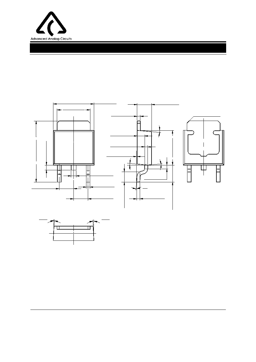
TO-252
3-TERMINAL 1A ADJUSTABLE VOLTAGE REGULATOR AZ317
Data Sheet
13
Apr. 2005 Rev. 1. 2
BCD Semiconductor Manufacturing Limited
Mechanical Dimensions (Continued)
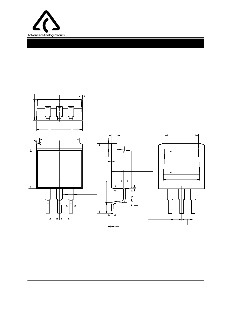
TO-263
Unit: mm(inch)
7
∞
3
∞
7
∞
8
.
6
4
0
(
0
.
3
4
0
)
9
.
6
5
0
(
0
.
3
8
0
)
0.990(0.039)
0.510(0.020)
2.540(0.100)
1.150(0.045)
9.650(0.380)
3
∞
14.760(0.581)
8.840(0.348)
2.640(0.104)
0.020(0.001)
8
∞
2
∞
0
∞
6
∞
0.380(0.015)
2
.
3
9
0
(
0
.
0
9
4
)
0.360(0.014)
2.200(0.087)
70
∞
10.290(0.405)
4.070(0.160)
4.820(0.190)
1.390(0.055)
1.150(0.045)
1.390(0.055)
2.540(0.100)
1.270(0.050)
1.390(0.055)
2
.
6
9
0
(
0
.
1
0
6
)
15.740(0.620)
0.250(0.010)
2.700(0.106)
0.400(0.016)
5
.
6
0
0
(
0
.
2
2
0
)
7.420(0.292)
7.980(0.314)
2.540(0.100)
2.540(0.100)

8F, B Zone, 900 Yi Shan Road, Shanghai 200233, PRC Tel: +86-21-6495 9539, Fax: +86-21-6485 9673
BCD Semiconductor (Taiwan) Company Limited
Room 2210, 22nd Fl, 333, Keelung Road, Sec. 1, TaiPei (110), Taiwan Tel: +886-2-2758 6828, Fax: +886-2-2758 6892
IMPORTANT NOTICE
BCD Semiconductor Manufacturing Limited reserves the right to make changes without further notice to any pro-
ducts or specifications herein. BCD Semiconductor Manufacturing Limited does not assume any responsibility for
use of any its products for any particular purpose, nor does BCD Semiconductor Manufacturing Limited assume any
liability arising out of the application or use of any its products or circuits. BCD Semiconductor Manufacturing Limi-
ted does not convey any license under its patent rights or other rights nor the rights of others.
http://www.bcdsemi.com
BCD Semiconductor Corporation
3170 De La Cruz Blvd, Suite # 105 Santa Clara, CA 95054-2411, U.S.A Tel: +1-408-988 6388, Fax: +1-408-988 6386
Shanghai SIM-BCD Semiconductor Manufacturing Co., Ltd.
800 Yi Shan Road, Shanghai 200233, PRC Tel: +86-21-6485-1491, Fax: +86-21-5450-0008
Advanced Analog Circuits (Shanghai) Corporation