Bel Fuse Inc.
206 Van Vorst Street, Jersey City, NJ 07302
∑ Tel 201-432-0463 ∑ Fax 201-432-9542 ∑ www.belfuse.com
NON-ISOLATED DC/DC CONVERTERS
8.3 V-14 V Input
0.75 V-5.0 V/6 A Output
∑ Non-Isolated
∑ Under-Voltage
Lockout
(UVLO)
∑ High
Efficiency
∑ OCP/SCP
∑ High
Power
Density
∑ Wide
Input
∑ Fixed
Frequency
∑ Wide
Trim
Range
∑ Remote
On/Off
∑ Active Low/High
∑ Flexible Output Voltage Sequencing
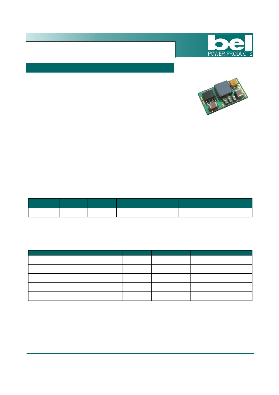
Description
The Bel SRBA-06A2Ax modules are a series of non-isolated dc/dc converters that deliver up to 6 A of output
current with full load efficiency of 92% at 5.0 V output. These modules provide precisely regulated voltage
programmable via external resistor from 0.75 V to 5.0 V over a wide range of input voltage (8.3 V-14 V). These
modules have a sequencing feature that enables designers to implement various types of output voltage
sequencing when powering multiple voltages on a board. The open-frame construction and small footprint
enable designers to develop cost and space-efficient solutions. Standard features include remote On/Off, over
current protection, short current protection, wide input, and programmable output voltage.
Part Selection
Output
Voltage
Input
Voltage
Max. Output
Current
Max. Output
Power
Typical
Efficiency
Model Number
Active Low
Model Number
Active High
0.75 V - 5.0 V
8.3 V - 14 V
6 A
30.0 W
92%
SRBA-06A2AL
SRBA-06A2A0
Note
: Add "G" suffix at the end of the model number to indicate Tray Packaging.
Absolute Maximum Ratings
Parameter
Min
Typ
Max
Notes
Input Voltage (continuous)
-0.3 V
-
15 V
Output Enable Terminal Voltage
-0.3 V
-
15 V
Sequencing Voltage
1
-0.3
V
-
Vin
Ambient Temperature
-40
∞C
-
85
∞C
Storage Temperature
-55
∞C
-
125
∞C
Notes
: All specifications are typical at 25
∞C unless otherwise stated.
1. SRBA-06A2Ax series of modules include a sequencing feature that enables users to implement
various types of output voltage sequencing in their applications. This is accomplished via an additional
sequencing pin. When the sequencing feature is not used, tie the SEQ pin to Vin.
SRBA-06A2Ax Series RoHS Compliant
Bel Fuse Inc.
206 Van Vorst Street, Jersey City, NJ 07302
∑ Tel 201-432-0463 ∑ Fax 201-432-9542 ∑ www.belfuse.com
NON-ISOLATED DC/DC CONVERTERS
8.3 V-14 V Input
0.75 V-5.0 V/6 A Output
Input Specifications
Parameter
Min
Typ
Max
Notes
Input Voltage
8.3 V
12 V
14 V
Input Current (full load)
Vo=5.0 V
Vo=3.3 V
Vo=2.5 V
Vo=1.8 V
Vo=1.2 V
Vo=0.75 V
-
-
-
-
-
-
2.75 A
1.85 A
1.45 A
1.05 A
0.75 A
0.55 A
4.0 A
2.8 A
2.2 A
1.6 A
1.1 A
0.8 A
Input Current (no load)
Vo=5.0 V
Vo=0.75 V
-
-
-
-
100 mA
20 mA
Remote Off Input Current
-
1 mA
2 mA
Input Reflected Ripple Current (pk-pk)
-
120 mA
-
Input Reflected Ripple Current (rms)
-
40 mA
-
Tested with two 100 uF/25 V tan input
capacitors & simulated source
impedance of 1 uH, 5 Hz to 20 MHz.
I
2
t Inrush Current Transient
-
0.002 A
2
s
0.02 A
2
s
Turn-on Voltage Threshold
-
8.1 V
8.2 V
Turn-off Voltage Threshold
-
7.5 V
8.0 V
Notes
: All specifications are typical at 25
∞C unless otherwise stated.
Output Specifications
Parameter
Min
Typ
Max
Notes
Output Voltage Set Point
-2%Vo,set
-
2%Vo,set
Vin=12 V, full load
Output Voltage Set Point
-2.5%Vo,set
-
3.5%Vo,set
Over all operating input
voltages, resistive loads and
temperature conditions
Adjustment Range Selected by
External Resistor or Voltage
0.7525 V
-
5.0 V
Load Regulation
-
0.4%Vo,set
-
Io=Io, min to Io, max
Line Regulation
-
0.3%Vo,set
-
Vin=Vin, min to Vin, max
Regulation Over Temperature
(-40
∞C to +85 ∞C)
-
0.5%Vo,set
-
Tref=Ta, min to Ta, max
Output Current
0 A
-
6 A
Current Limit Threshold
7.2 A
-
18 A
Short Circuit Surge Transient
- 0.25
A
2
s -
Ripple and Noise (pk-pk)
Vo=0.75 V-3.63 V
-
50 mV
75 mV
Ripple and Noise (rms)
Vo=0.75 V-3.63 V
-
15 mV
30 mV
Ripple and Noise (pk-pk)
Vo=5.0 V
-
75 mV
100 mV
Ripple and Noise (rms)
Vo=5.0 V
-
30 mV
40 mV
Tested with 0-20 MHz, with
10 uF/10 V tantalum
capacitor & 1 uF/10 V TDK
ceramic capacitor at the
output.
Turn on Time
-
8 mS
10 mS
Overshoot at Turn on
-
0%
3%
Output Capacitance
ESR
1 mohm
ESR
10 mohm
0 uF
0 uF
-
-
1000 uF
3000 uF
Bel Fuse Inc.
206 Van Vorst Street, Jersey City, NJ 07302
∑ Tel 201-432-0463 ∑ Fax 201-432-9542 ∑ www.belfuse.com
NON-ISOLATED DC/DC CONVERTERS
8.3 V-14 V Input
0.75 V-5.0 V/6 A Output
Output Specifications (Continued)
Parameter
Min
Typ
Max
Notes
Transient Response
50% ~ 100% Max Load
-
200 mV
-
Settling Time
-
50 uS
-
100% ~ 50% Max Load
-
200 mV
-
Settling Time
V
O
=
0.75 - 5 V
- 50
uS
-
di/dt=2.5 A/uS; Vin=12 V;
and with 10 uF/10 V
tantalum capacitor & 1 uF/
10 V ceramic capacitor at the
output.
Note
: All specifications are typical at nominal input (Vin=12 V), full load at 25
∞C
unless otherwise stated.
General Specifications
Parameter
Min
Typ
Max
Notes
Efficiency
Vo=5.0 V
Vo=3.3 V
Vo=2.5 V
Vo=1.8 V
Vo=1.2 V
Vo=0.75 V
90%
87%
85%
83%
79%
71%
92%
89%
88%
86%
82%
74%
-
-
-
-
-
-
Measured at Vin=12 V, full load
Switching Frequency
250 kHz
300 kHz
350 kHz
Over Temperature Shutdown
-
135
∞C
-
Output Trim Range (wide trim)
0.7525 V
-
5 V
MTBF
3,079,469 hours
Calculated Per Bell Core SR-332 (I
O
=
Nominal; T
a
= 25
∞C)
Dimensions
Inches (L ◊ W ◊ H)
Millimeters (L ◊ W ◊ H)
0.8 x 0.45 x 0.251
20.32 x 11.42 x 6.38
Weight -
3
g
-
Note
: All specifications are typical at 25
∞C
unless otherwise stated.
Control Specifications
Parameter
Min
Typ
Max
Notes
Signal Low (Unit Off)
-0.3 V
-
0.4 V
Signal High (Unit On)
2.5 V
-
14 V
SRBA-06A2A0; Remote On/Off pin open, Unit
on.
Signal Low (Unit On)
-0.3 V
-
0.4 V
Signal High (Unit Off)
2.5 V
-
14 V
SRBA-06A2AL; Remote On/Off pin open, Unit
on.
Sequencing Voltage
0 V
-
Vin
Sequencing Voltage applied on SEQ pin
should be higher than output voltage.
Sequencing Slew Rate Capability
-
-
2 V/mS
Sequencing Delay Time
10 mS
-
-
Delay from Vin, min to application of voltage
on SEQ pin
Tracking Accuracy
Power-Up
Power-Down
-
-
100 mV
200 mV
200 mV
400 mV
Bel Fuse Inc.
206 Van Vorst Street, Jersey City, NJ 07302
∑ Tel 201-432-0463 ∑ Fax 201-432-9542 ∑ www.belfuse.com
NON-ISOLATED DC/DC CONVERTERS
8.3 V-14 V Input
0.75 V-5.0 V/6 A Output
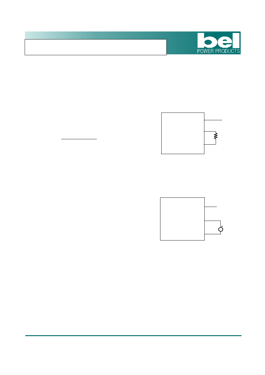
Output Trim Equations
Equation for calculating the trim resistor (in k) given the desired adjusted voltage (Vadj) is shown below. The
Trim Up resistor should be connected between the Trim pin and Ground.
1
7525
.
0
507
.
10
-
-
=
adj
trim
V
R
Equation for calculating the trim voltage (in V) given the desired adjusted voltage (Vadj) is shown below. The
Trim Up voltage should be connected between the Trim pin and Ground.
)
7525
.
0
(
0667
.
0
7
.
0
-
◊
-
=
adj
trim
V
V
Rtrim
Module
Vout
GND
Trim
Vtrim
Module
Vout
GND
Trim
Bel Fuse Inc.
206 Van Vorst Street, Jersey City, NJ 07302
∑ Tel 201-432-0463 ∑ Fax 201-432-9542 ∑ www.belfuse.com
NON-ISOLATED DC/DC CONVERTERS
8.3 V-14 V Input
0.75 V-5.0 V/6 A Output
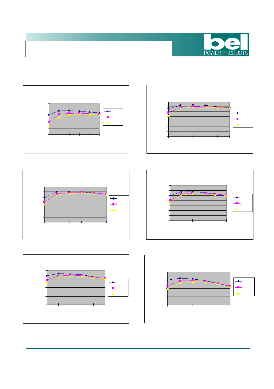
Efficiency Data
MODULE 5.0V
75.0%
80.0%
85.0%
90.0%
95.0%
100.0%
1A
2A
3A
4A
5A
6A
OUTPUT CURRENT
EFF
I
C
I
EN
CY
8.3V
12.0V
14.0V
MODULE 3.3V
60.0%
65.0%
70.0%
75.0%
80.0%
85.0%
90.0%
95.0%
1A
2A
3A
4A
5A
6A
OUTPUT CURRENT
EF
F
I
CI
ENCY
8.3V
12.0V
14.0V
MODULE 2.5V
60.0%
65.0%
70.0%
75.0%
80.0%
85.0%
90.0%
95.0%
1A
2A
3A
4A
5A
6A
OUTPUT CURRENT
EF
F
I
CI
EN
CY
8.3V
12.0V
14.0V
MODULE 1.8V
60.0%
65.0%
70.0%
75.0%
80.0%
85.0%
90.0%
95.0%
1A
2A
3A
4A
5A
6A
OUTPUT CURRENT
EFFI
CI
EN
C
Y
8.3V
12.0V
14.0V
MODULE 1.2V
50.0%
60.0%
70.0%
80.0%
90.0%
1A
2A
3A
4A
5A
6A
OUTPUT CURRENT
EF
F
I
CI
E
N
CY
8.3V
12.0V
14.0V
MODULE 0.75V
50.0%
60.0%
70.0%
80.0%
90.0%
1A
2A
3A
4A
5A
6A
OUTPUT CURRENT
EFF
I
C
I
EN
C
Y
8.3V
12.0V
14.0V