Äîêóìåíòàöèÿ è îïèñàíèÿ www.docs.chipfind.ru
Bel Fuse Inc.
206 Van Vorst Street, Jersey City, NJ 07302
· Tel 201-432-0463 · Fax 201-432-9542 · www.belfuse.com
NON-ISOLATED DC/DC CONVERTERS
8.3 V-14 V Input
0.75 V-5.5 V/16 A Output
· Non-Isolated
· Under-voltage
Lockout
(UVLO)
· High
Efficiency
· Over
Temperature
Protection
· High
Power
Density
· OCP/SCP
· Excellent Thermal Performance
· Wide
Input
· Low
Cost
· Wide
Trim
· Flexible Output Voltage
Sequencing (option)
· Remote
On/Off
· Active
Low/High
(option)
· Able to Sink & Source Current
· Vout
Prebias
· Remote
Sense
· Industrial Temperature Range
Description
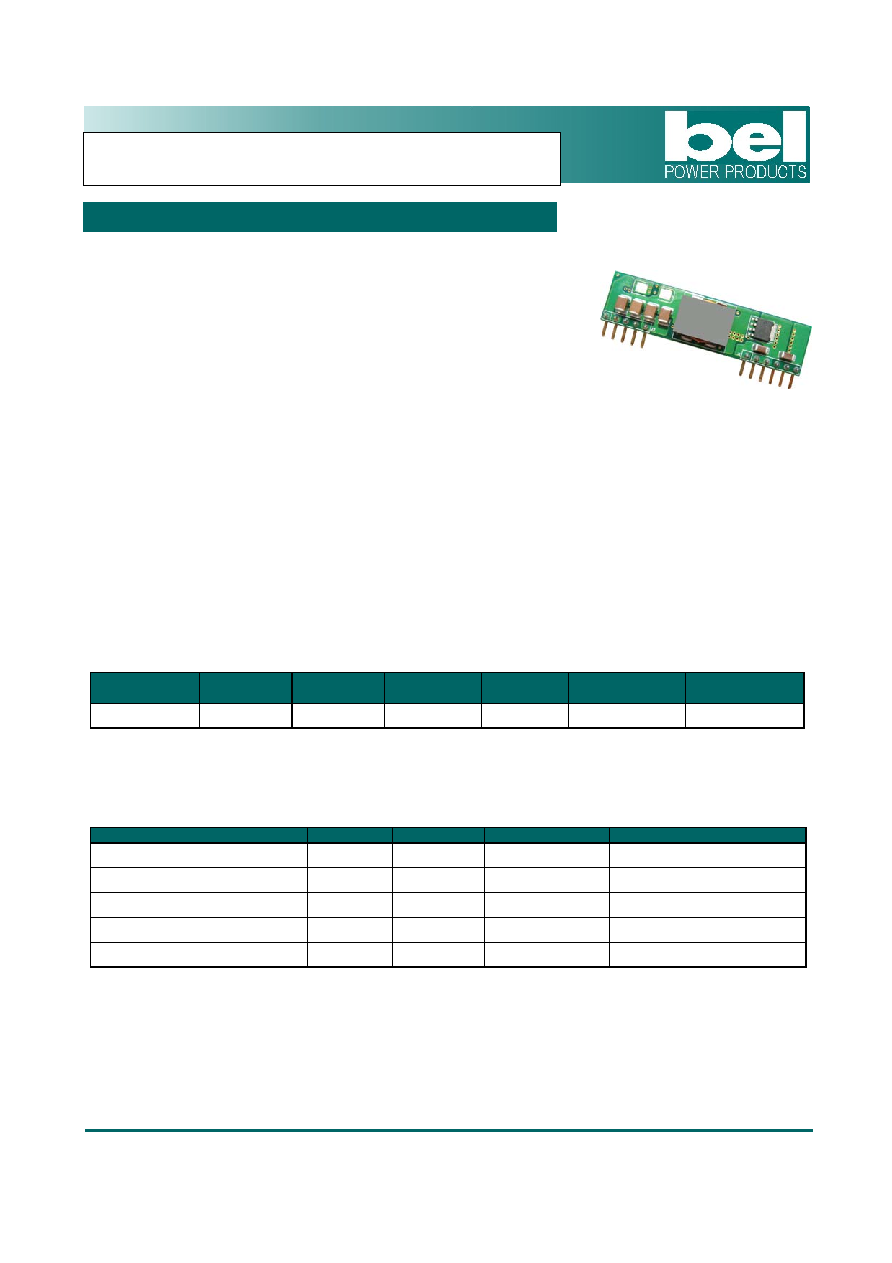
The Bel VRBC-16A2Ax is part of the non-isolated dc/dc converter series. The modules use a SIP package.
These converters are available in a range of output voltages from 0.75 V to 5.5 V over a wide range of input
voltage (Vin = 8.3 V-14 V). The Bel VRBC-16A2Ax has a sequencing feature that enables designers to
implement various types of output voltage sequencing when powering. The efficiency is typically 92% at 3.3 V
output and 12 V input at full load.
Part Selection
Output
Voltage
Input
Voltage
Max. Output
Current
Max. Output
Power
Typical
Efficiency
Model Number
Active Low
Model Number
Active High
0.75 V - 5.5 V
8.3 V - 14 V
16 A
80 W
94%
VRBC-16A2AL
VRBC-16A2A0
Notes:
1.Change the last character to "C" to indicate 0.20'' pin length and active low.
2. Add "G" suffix at the end of the model number to indicate Tray Packaging.
Absolute Maximum Ratings
Parameter
Min
Typ
Max
Notes
Input Voltage (continuous)
-0.3 V
-
15 V
Output Enable Terminal Voltage
-0.3 V
-
15 V
Sequencing Voltage
1
-0.3
V
-
Vin
Ambient Temperature
-40
°C
-
85
°C
Storage Temperature
-55
°C
-
125
°C
Notes
: All specifications are typical at 25
°C
unless otherwise stated.
1. VRBC-16A2Ax series of modules include a sequencing feature that enables users to implement
various types of output voltage sequencing in their applications. This is accomplished via an additional
sequencing pin. When not using the sequencing feature, either, tie the SEQ pin to Vin or leave it
unconnected.
VRBC-16A2Ax Series RoHS Compliant
Bel Fuse Inc.
206 Van Vorst Street, Jersey City, NJ 07302
· Tel 201-432-0463 · Fax 201-432-9542 · www.belfuse.com
NON-ISOLATED DC/DC CONVERTERS
8.3 V-14 V Input
0.75 V-5.5 V/16 A Output
Input Specifications
Parameter
Min
Typ
Max
Notes
Input Voltage
Vo, set3.63 V
Vo, set
>
3.63 V
8.3 V
8.3 V
12 V
12 V
14 V
13.2 V
Input Current (full load)
-
-
11 A
Input Current (no load)
-
100 mA
-
Remote Off Input Current
-
2 mA
-
Input Reflected Ripple Current (pk-pk)
-
30 mA
-
Tested with one 1000 uF/25 V AL input
capacitor with ESR=0.03 ohm max and
6 × 47uF/16 V tan capacitors with
ESR=0.013 ohm max at 100 kHz, &
simulated source impedance of 1000
nH, 5 Hz to 20 MHz.
I
2
t Inrush Current Transient
-
0.2 A
2
s 0.4
A
2
s
Turn-on Voltage Threshold
-
7.8 V
-
Turn-off Voltage Threshold
-
7.3 V
-
Output Specifications
Parameter
Min
Typ
Max
Notes
Output Voltage Set Point
-2% Vo,set
-
2% Vo,set
Vin=12 V, full load
Load Regulation
-
0.4% Vo,set
-
Io=Io, min to Io, max
Line Regulation
-
0.3% Vo,set
-
Vin=Vin, min to Vin, max
Regulation Over Temperature
(-40
°C to +85°C)
-
0.4% Vo,set
-
Tref=Ta, min to Ta, max
Output Current
0 A
-
16 A
Current Limit Threshold
- 180%
Io,out
-
Short Circuit Surge Transient
- 1
A
2
s 3
A
2
s
Ripple and Noise (pk-pk)
-
50 mV
100 mV
Ripple and Noise (rms)
-
30 mV
45 mV
Tested with 0-20 MHz, 10 uF
Tantalum capacitor &1 uF
ceramic capacitor at the output
Turn on Time
-
8 mS
20 mS
Overshoot at Turn on
-
-
1% Vo,set
0 uF
-
5000 uF
ESR10 mohm
Output Capacitance
0 uF
-
1000 uF
ESR1 m
Transient Response
50% ~ 100% Max Load
-
100 mV
-
Settling Time
-
80 uS
-
100% ~ 50% Max Load
-
100 mV
-
Settling Time
All
- 80
uS
-
di/dt=2.5 A/uS; Vin=12 V; and
with 330uF Tantalum
capacitors at the output
Note
: All specifications are typical at nominal input, full load at 25
°C
unless otherwise stated.
Bel Fuse Inc.
206 Van Vorst Street, Jersey City, NJ 07302
· Tel 201-432-0463 · Fax 201-432-9542 · www.belfuse.com
NON-ISOLATED DC/DC CONVERTERS
8.3 V-14 V Input
0.75 V-5.5 V/16 A Output
General Specifications
Parameter
Min
Typ
Max
Notes
Efficiency
Vo=5.0 V
Vo=3.3 V
Vo=2.5 V
Vo=1.8 V
Vo=1.5 V
Vo=1.2 V
Vo=0.75 V
-
-
-
-
-
-
-
94%
92%
90%
88%
87%
85%
78%
-
-
-
-
-
-
-
Measured at Vin=12 V, full load
Switching Frequency
250 kHz
280 kHz
310 kHz
Over Temperature Shutdown
1
-
130
°C
-
Output Trim Range (Wide Trim)
0.7525 V
-
5.5 V
Remote Sense Compensation
-
-
0.5 V
MTBF
4,619,490 hours
Calculated Per Bell Core SR-332 (I
O
= 80%
Io,max; Vin=12 V; Vo=3.3 V; T
a
= 25
°C)
Dimensions
Inches (L × W × H)
Millimeters (L × W × H)
2.0x 0.5 x 0.32
50.8 x 12.7 x 8.13
Weight -
7.1
g
-
Notes
: All specifications are typical at 25
°C
unless otherwise stated.
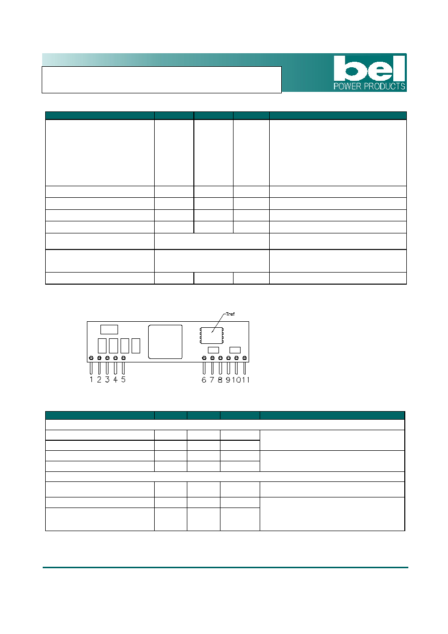
1. The Tref temperature measurement location:
Control Specifications
Parameter
Min
Typ
Max
Notes
Remote On/Off
Signal Low (Unit Off)
-0.2 V
-
0.3 V
Signal High (Unit On)
-
-
Vin, max
VRBC-16A2A0; Remote On/Off pin open, Unit
on.
Signal Low (Unit On)
-0.2 V
-
0.3 V
Signal High (Unit Off)
2.5 V
-
Vin, max
VRBC-16A2AL; Remote On/Off pin open, Unit
on.
Voltage Sequencing
Sequencing Delay Time
10 mS
-
-
Delay from Vin, min to application of voltage
on SEQ pin
Sequencing Slew Rate Capability
-
-
2 V/mS
Tracking Accuracy
Power-Up
Power-Down
-
-
100 mV
300 mV
200 mV
500 mV
Vin, min to Vin, max; Io, min to Io, max;
Vseq<Vo
Bel Fuse Inc.
206 Van Vorst Street, Jersey City, NJ 07302
· Tel 201-432-0463 · Fax 201-432-9542 · www.belfuse.com
NON-ISOLATED DC/DC CONVERTERS
8.3 V-14 V Input
0.75 V-5.5 V/16 A Output
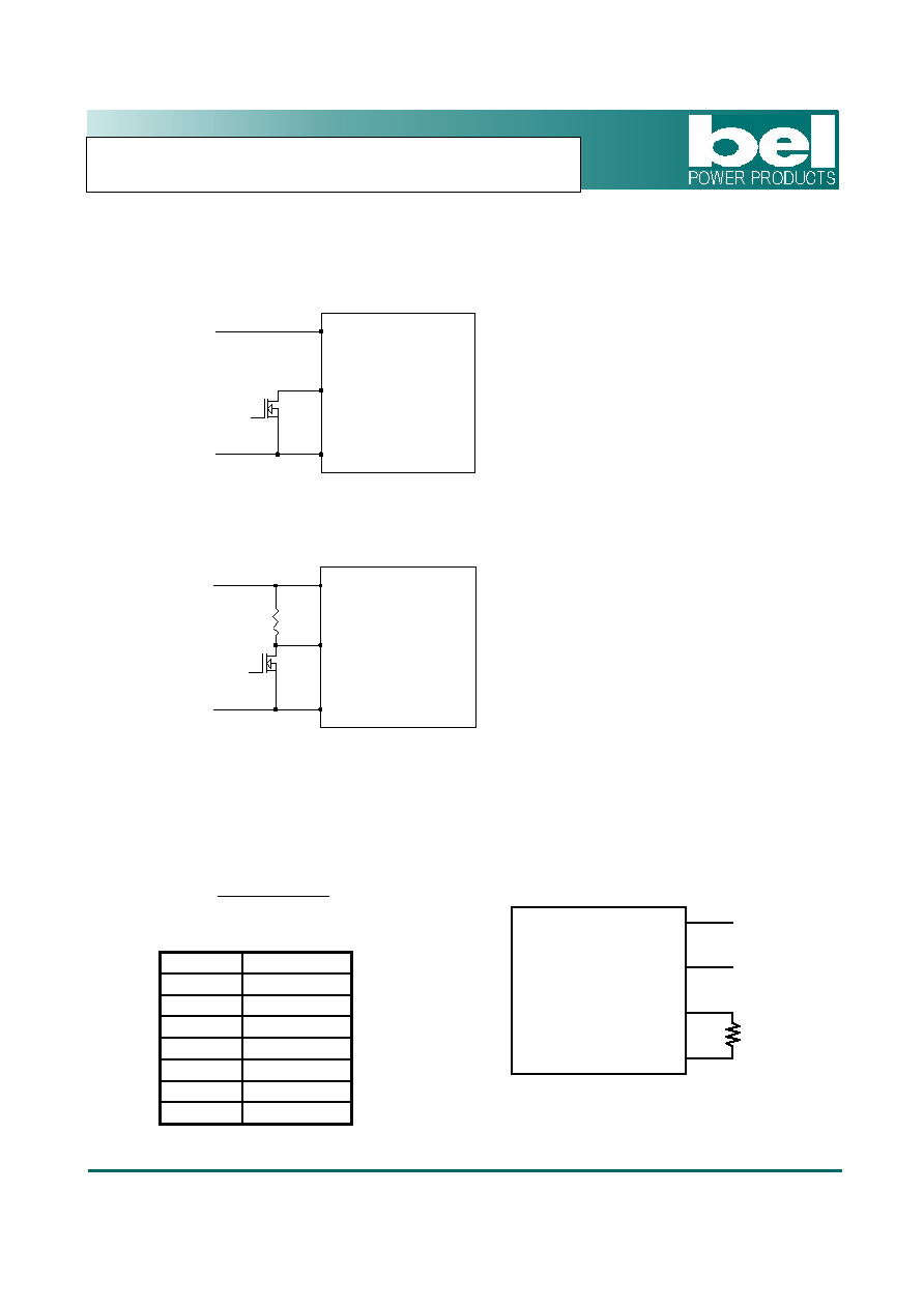
Remote On/Off
For Active High Modules (Positive Logic)
When the transistor Q1 is in the Off state, the power module is ON.
When the transistor Q1 is turned On, the power module is OFF.
For Active Low Modules (Negative Logic)
When the transistor Q1 is in the Off state, the power module is OFF.
When the transistor Q1 is turned On, the power module is ON.
Output Trim Equations
Equation for calculating the trim resistor given the desired output voltage (Vo) is shown below. The Trim Up
resistor should be connected between the Trim pin and Ground.
( )
-
-
=
1000
7525
.
0
10500
Vo
R
trim
Vo (V)
Rtrim (K)
0.7525 Open
1.2 22.46
1.5 13.05
1.8 9.024
2.5 5.009
3.3 3.122
5.0
1.472
Rtrim
Module
Vout
GND
Sense
trim
Remote On/Off
GND
Vin
Q1
GND
Vin
Module
R
Remote On/Off
GND
Vin
Q1
GND
Vin
Module
Bel Fuse Inc.
206 Van Vorst Street, Jersey City, NJ 07302
· Tel 201-432-0463 · Fax 201-432-9542 · www.belfuse.com
NON-ISOLATED DC/DC CONVERTERS
8.3 V-14 V Input
0.75 V-5.5 V/16 A Output
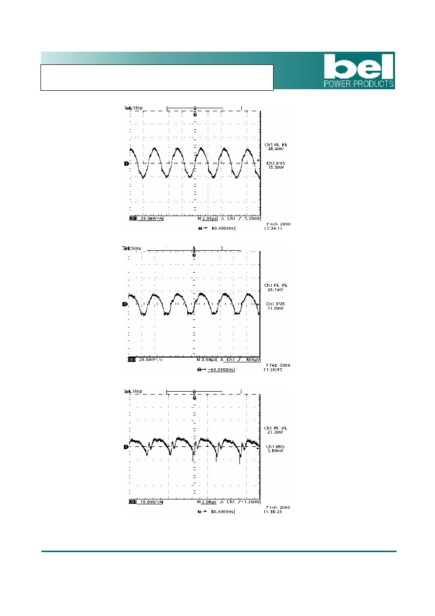
Ripple and Noise
Ripple and noise at full load, 12Vdc input, 5.0V output and Ta=25 deg C
Ripple and noise at full load, 12Vdc input, 3.3V output and Ta=25 deg C
Ripple and noise at full load, 12Vdc input, 0.75V output and Ta=25 deg C
Note:
External load with 10uF tantalum capacitor and 1uF ceramic at the output.