Continental Device India Limited
An IS/ISO 9002 and IECQ Certified Manufacturer
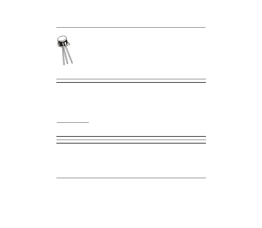
NPN SILICON PLANAR TRANSISTOR
2N2484
TO-18
This transistors is primarily intended for use in high performance, low level,
low noise amplifier applications
ABSOLUTE MAXIMUM RATINGS
DESCRIPTION
SYMBOL
VALUE
UNIT
Collector -Emitter Voltage
VCEO
60
V
Collector -Base Voltage
VCBO
60
V
Emitter -Base Voltage
VEBO
6.0
V
Collector Current Continuous
IC
50
mA
Power Dissipation @Ta=25 degC
PD
360
mW
Derate Above 25 deg C
2.06
mw/deg C
Power Dissipation @Tc=25 degC
PD
1.20
W
Derate Above 25 deg C
6.85
mw/deg C
Operating And Storage Junction
Tj, Tstg
-65 to +200
deg C
Temperature Range
THERMAL RESISTANCE
Junction to Case
Rth(j-c)
146
deg C/W
Junction to Ambient in Free Air
Rth(j-a) *
485
deg C/W
Lead Temperature
TL
300
deg C
1/16" from Case for 10 Seconds
ELECTRICAL CHARACTERISTICS (Ta=25 deg C Unless Otherwise Specified)
DESCRIPTION
SYMBOL
TEST CONDITION
Min
MAX UNIT
Collector -Emitter Voltage
VCEO**
IC=10mA,IB=0
60
-
V
Collector -Base Voltage
VCBO
IC=10uA.IE=0
60
-
V
Emitter -Base Voltage
VEBO
IE=10uA, IC=-0
6.0
-
V
Collector-Cut off Current
ICBO
VCB=45V, IE=0
-
10
nA
Ta=150 deg C
VCB=45V, IE=0
-
10
uA
Emitter-Cut off Current
IEBO
VEB=5V, IC=0
-
10
nA
Collector Emitter Saturation Voltage
VCE(Sat)
IC=1mA,IB=0.1mA
-
0.35
V
Base Emitter on Voltage
VBE(on)
IC=0.1mA, VCE=5V
0.5
0.7
V
IS/ISO 9002
Lic# QSC/L- 000019.2
IS / IECQC 700000
IS / IECQC 750100
Continental Device India Limited
Data Sheet
Page 1 of 3
Boca Semiconductor Corp
BSC
http://www.bocasemi.com page : 1

ELECTRICAL CHARACTERISTICS (Ta=25 deg C Unless Otherwise Specified)
2N2484
DESCRIPTION
SYMBOL
TEST CONDITION
MIN
MAX
UNIT
DC Current Gain
hFE
IC=1uA, VCE=5V
30
-
IC=10uA, VCE=5V
100
500
Ta=55 deg C
IC=10uA, VCE=5V
20
-
IC=100uA, VCE=5V
175
-
IC=500uA, VCE=5V
200
-
IC=1mA, VCE=5V
250
-
IC=10mA,VCE=5V**
-
800
Dynamic Characteristics
Transition Frequency
ft
VCE=5V,IC=0.05mA
15
-
MHz
f=5MHz
VCE=5V,IC=0.5mA,
60
-
MHz
f=30MHz
Out-put Capacitance
Cobo
VCB=5V, IE=0
-
6.0
pF
f=140kHz
In-put Capacitance
Cibo
VEB=0.5V, IC=0
-
6.0
pF
f=140kHz
Noise Figure
NF
VCE=5V, IC=10uA
Rs=10kohms
f=100Hz, BW'=20Hz
-
10
dB
f=1kHz, BW=200Hz
-
3.0
dB
f=10kHz, BW=2kHz
-
2.0
dB
f=10Hz to 15.7kHz,BW=15.7KHz
3.0
dB
Small Signal Characteristics (@ f=1kHz unless otherwise specified)
Input Impedence
hie
IC=1mA, VCE=5V
3.5
24
kohms
-4
Voltage Feedback Ratio
hre
IC=1mA, VCE=5V
-
800
x10
Small Signal Current Gain
hfe
IC=1mA, VCE=5V
150
900
Output Admittance
hoe
IC=1mA, VCE=5V
-
40
umhos
*Rth(j-a) is measured with the device soldered into a typical printed Circuit board.
**Pulse Test: Pulse Width=300us, Duty Cycle=2%
Continental Device India Limited
Data Sheet
Page 2 of 3
http://www.bocasemi.com page : 2
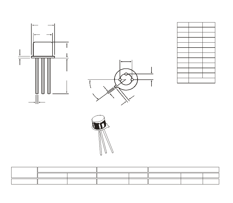
TO-18 Metal Can Package
Disclaimer
TO-18
1K/polybag
350 gm/1K pcs
3" x 7.5" x 7.5"
5.0K
17" x 15" x 13.5"
80.0K
34 kgs
PACKAGE
Net Weight/Qty
Details
STANDARD PACK
INNER CARTON BOX
Qty
OUTER CARTON BOX
Qty
Gr Wt
Size
Size
Packing Detail
G
1
2
3
H
J
L
F
A
D
B
E
C
K
DIM
M IN
M A X
A
l
l
d
i
m
i
ns
i
ons
i
n
m
m
.
A
5.24
5.84
B
4.52
4.97
C
4.31
5.33
D
0.40
0.53
E
--
0.76
F
--
1.27
G
--
2.97
H
0.91
1.17
J
0.71
1.21
K
12.70
--
L
45 DE G
PIN CONFIGURATION
1. EM ITTER
2. BASE
3. COLLECTOR
1
2
3
The product information and the selection guides facilitate selection of the CDIL's Discrete Semiconductor Device(s) best suited
for application in your product(s) as per your requirement. It is recommended that you completely review our Data Sheet(s) so as
to confirm that the Device(s) meet functionality parameters for your application. The information furnished on the CDIL Web
Site/CD is believed to be accurate and reliable. CDIL however, does not assume responsibility for inaccuracies or incomplete
information. Furthermore, CDIL does not assume liability whatsoever, arising out of the application or use of any CDIL product;
neither does it convey any license under its patent rights nor rights of others. These products are not designed for use in life
saving/support appliances or systems. CDIL customers selling these products (either as individual Discrete Semiconductor
Devices or incorporated in their end products), in any life saving/support appliances or systems or applications do so at their own
risk and CDIL will not be responsible for any damages resulting from such sale(s).
CDIL strives for continuous improvement and reserves the right to change the specifications of its products without prior notice.
CDIL is a registered Trademark of
Continental Device India Limited
C-120 Naraina Industrial Area, New Delhi 110 028, India.
Telephone + 91-11-579 6150 Fax + 91-11-579 9569, 579 5290
e-mail sales@cdil.com www.cdil.com
Continental Device India Limited
Data Sheet
Page 3 of 3
http://www.bocasemi.com page : 3