 | –≠–ª–µ–∫—Ç—Ä–æ–Ω–Ω—ã–π –∫–æ–º–ø–æ–Ω–µ–Ω—Ç: KA79L05A | –°–∫–∞—á–∞—Ç—å:  PDF PDF  ZIP ZIP |

©2001 Fairchild Semiconductor Corporation
www.fairchildsemi.com
Rev. 1.0.1
Features
∑ Output current up to 100mA
∑ No external components
∑ Internal thermal over load protection
∑ Internal short circuit current limiting
∑ Output Voltage Offered in
±
5% Tolerance
∑ Output Voltage of -5V, -8V, -12V, -15V, -18V
and -24V
Description
These regulators employ internal current limiting and ther-
mal shutdown, making them essentially indestructible.
TO-92
1.GND 2.Input 3.Output
1
8-SOP
SOT-89
1
1
1. Output 2.3.6.7. GND 4.5. NC 8. Input
Internal Block Diagram
Output
Input
KA79LXXA
3-Terminal 0.1A Negative Voltage Regulator
Boca Semiconductor Corp.
BSC
http://www.bocasemi.com
http://www.bocasemi.com

KA79LXXA
2
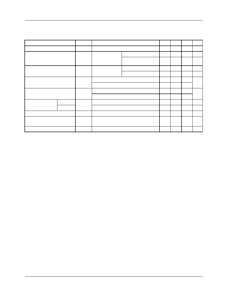
Absolute Maximum Ratings
Electrical Characteristics(KA79L05A)
(V
I
= -10V, I
O
= 40mA, C
I
= 0.33
µ
F, C
O
= 0.1
µ
F, 0
∞
C
T
J
+125
∞
C, unless otherwise specified)
Note
1. Load and line regulation are specified at constant junction temperature. Change in V
O
due to heating effects must be taken
into account separately. Pulse testing with low duty is used.
Parameter
Symbol
Value
Unit
Input Voltage (for V
o
= -5V to -8V)
(for V
o
= -12V to -18V)
(for V
o
= -24V)
V
I
-30
-35
-40
V
Operating Temperature Range
T
OPR
0 ~ +125
∞
C
Storage Temperature Range
T
STG
-65 ~ +150
∞
C
Parameter
Symbol
Conditions
Min.
Typ. Max.
Unit
Output Voltage
V
O
T
J
= +25
∞
C
- 4.8 - 5.0
- 5.2
V
Line Regulation (Note1)
V
O
T
J
=+25
∞
C
-7.0V
V
I
-20V
-
15
150
mV
-8V
V
I
-20V
-
-
100
mV
Load Regulation (Note1)
V
O
T
J
=+25
∞
C
1.0mA
I
O
100mA
-
20
60
mV
1.0mA
I
O
40mA
-
10
30
mV
Output Voltage
V
O
-7.0V
V
I
-20V, 1.0mA
I
O
40mA - 4.75
-
- 5.25
V
V
I
= -10V, 1.0mA
I
O
70mA
- 4.75
-
- 5.25
V
Quiescent Current
I
Q
T
J
=+ 25
∞
C
-
2.0
5.5
mA
T
J
= +125
∞
C
-
-
6.0
Quiescent Current
Change
with line
I
Q
-8V
V
I
-20V
-
-
1.5
mA
with load
I
Q
1.0mA
I
O
40mA
-
-
0.1
mA
Output Noise Voltage
V
N
T
A
= +25
∞
C,10Hz
f
100KHz
-
30
-
µ
V
Ripple Rejection
RR
f = 120Hz, -8V
V
I
-18V
T
J
= +25
∞
C
41
60
-
dB
Dropout Voltage
V
D
T
J
= +25
∞
C
-
1.7
-
V
KA79LXXA
3
Electrical Characteristics (KA79L08A)
(V
I
= -14V, I
O
= 40mA, C
I
= 0.33
µ
F, C
O
= 0.1
µ
F, 0
∞
C
T
J
+125
∞
C, unless otherwise specified)
Note
1. Load and line regulation are specified at constant junction temperature. Change in V
O
due to heating effects must be taken
into account separately. Pulse testing with low duty is used.
Parameter
Symbol
Conditions
Min.
Typ. Max. Unit
Output Voltage
V
O
T
J
= +25
∞
C
- 7.7 - 8.0
- 8.3
V
Line Regulation (Note1)
V
O
T
J
=+25
∞
C
-10.3V
V
I
-23V
-
-
175
mV
-12V
V
I
-23V
-
-
125
mV
Load Regulation (Note1)
V
O
T
J
=+25
∞
C
1.0mA
I
o
100mA
-
-
80
mV
1.0mA
I
o
40mA
-
-
40
mV
Output Voltage
V
O
-10.3V
V
I
-23V, 1.0mA
I
o
40mA
- 7.6
-
- 8.4
V
V
I
= -14V, 1.0mA
I
o
70mA
- 7.6
-
- 8.4
Quiescent Current
I
Q
T
j
=+ 25
∞
C
-
-
6.0
mA
T
j
= +125
∞
C
-
-
5.5
Quiescent Current
Change
with line
I
Q
-11.7V
V
I
-23V
-
-
1.5
mA
with load
1.0mA
I
o
40mA
-
-
0.1
mA
Output Noise Voltage
V
N
T
j
= +25
∞
C,10Hz
f
100KHz
-
50
-
µ
V
Ripple Rejection
RR
f = 120Hz, -11V
V
I
-21V
T
j
= +25
∞
C
39
55
-
dB
Dropout Voltage
V
D
T
j
= +25
∞
C
-
1.7
-
V

KA79LXXA
4
Electrical Characteristics(KA79L12A)
(V
I
= -19V, I
O
= 40mA, C
I
= 0.33
µ
F, C
O
= 0.1
µ
F, 0
∞
C
T
J
+125
∞
C, unless otherwise specified)
Note
1. Load and line regulation are specified at constant junction temperature. Change in V
O
due to heating effects must be taken
into account separately. Pulse testing with low duty is used.
Parameter
Symbol
Conditions
Min.
Typ. Max.
Unit
Output Voltage
V
O
T
J
= +25
∞
C
-11.5 -12.0 -12.5
V
Line Regulation (Note1)
V
O
T
J
= +25
∞
C
-14.5V
V
I
-27V
-
-
250
mV
-16V
V
I
-27V
-
-
200
mV
Load Regulation (Note1)
V
O
T
J
= +25
∞
C
1.0mA
I
O
100mA
-
-
100
mV
1.0mA
I
O
40mA
-
-
50
mV
Output Voltage
V
O
-14.5V
>
V
I
>
-27V, 1.0mA
I
O
40mA -11.4
-
-12.6
V
V
I
= -19V, 1.0mA
I
O
70mA
-11.4
-
-12.6
V
Quiescent Current
I
Q
T
J
= +25
∞
C
-
-
6.0
mA
T
J
= +125
∞
C
-
-
6.5
Quiescent Current
Change
with line
I
Q
-16V
V
I
-27V
-
-
1.5
mA
with load
I
Q
1.0mA
I
O
40mA
-
-
0.1
mA
Output Noise Voltage
V
N
T
A
= +25
∞
C,10Hz
f
100KHz
-
80
-
µ
V
Ripple Rejection
RR
f = 120Hz, -15V
V
I
-25V
T
J
= +25
∞
C
37
42
-
dB
Dropout Voltage
V
D
T
J
= +25
∞
C
-
1.7
-
V

KA79LXXA
5
Electrical Characteristics(KA79L15A)
(V
I
= -23V, I
O
= 40mA, C
I
= 0.33
µ
F, C
O
= 0.1
µ
F, 0
∞
C
T
J
+125
∞
C, unless otherwise specified)
Note
1. Load and line regulation are specified at constant junction temperature. Change in V
O
due to heating effects must be taken
into account separately. Pulse testing with low duty is used.
Parameter
Symbol
Conditions
Min.
Typ.
Max. Unit
Output Voltage
V
O
T
J
= +25
∞
C
-14.4 -15.0 -15.6
V
Line Regulation (Note1)
V
O
T
J
= +25
∞
C
-17.5V
V
I
-30V
-
-
300
mV
-20V
V
I
-30V
-
-
250
mV
Load Regulation (Note1)
V
O
T
J
= +25
∞
C
1.0mA
I
O
100mA
-
-
150
mV
1.0mA
I
O
40mA
-
-
75
mV
Output Voltage
V
O
-17.5V
V
I
-30V, 1.0mA
I
O
40mA
-14.25
-
-15.75
V
V
I
= -23V, 1.0mA
I
O
70mA
-14.25
-
-15.75
V
Quiescent Current
I
Q
T
J
= +25
∞
C
-
-
6.0
mA
T
J
= +125
∞
C
-
-
6.5
Quiescent Current
Change
with line
I
Q
-20V
V
I
-30V
-
-
1.5
mA
with load
I
Q
1.0mA
I
O
40mA
-
-
0.1
mA
Output Noise Voltage
V
N
T
A
= +25
∞
C,10Hz
f
100KHz
-
90
-
µ
V
Ripple Rejection
RR
f = 120Hz, -18.5V
V
I
-28.5V
T
J
= +25
∞
C
34
39
-
dB
Dropout Voltage
V
D
T
J
= +25
∞
C
-
1.7
-
V