Data
sheet
www.bookham.com
Thinking optical solutions
www.bookham.com
Thinking optical solutions
Features
∑ DWDM 2.5 Gb/s optical
transmitter and APD receiver
∑ C band operation (100 GHz
spacing) with integrated
Etalon locker
∑ High optical output power,
+4 dBm
∑ Very low power dissipation,
1 W typical
∑ Single supply rail, +3.3 V
∑ Supports serial line rates from
50 Mb/s to 2.7 Gb/s (OC3,
OC12, GE, OC48,
and OC48+FEC)
∑ 1550 nm b-HET directly
modulated laser for reaches
up to 175km and 360km
∑ APD pre-amp receiver for
excellent sensitivity, -28dBm EOL
∑ Micro controller with I
2
C interface
for wavelength locking, control,
and alarms
∑ Compliant with Telcordia GR-253,
ITU-T G.691, G.692, G.783,
and G.957
∑ Case operating temperature
range +0∞C to +70∞C
2.5 Gb/s DWDM
Transceiver Module
The Bookham Technology MQ25EW 2.5 Gb/s DWDM Transceiver Module
is a very low power, small form factor module enabling high port density. It
is designed to provide a SONET OC48/SDH STM-16 compliant interface
between the photonic layer and the electrical layer for applications
requiring up to 175km and 360km reach. This module
is compliant to the DWDM Hot-pluggable MSA.
Typical power dissipation of 2.2 W coupled with the small footprint significantly
simplifies card design. This results
in significant savings in card space and development time,
and greatly improved time to market.
The module provides wavelengths on the 100 GHz ITU grid in the C band. A
two-wire communication interface (I
2
C) is available for extended monitoring and
alarm information to complement the hardware alarms and monitors. These
include bias and modulation current, power, wavelength, laser and APD
temperature, LOS, and APD photocurrent.
The MQ25EW 2.5 Gb/s DWDM Transceiver module can be used for existing
OC48 as well as emerging Gigabit Ethernet ports. The MQ25EW is optimized for
links spans of up to 360km using an APD receiver.
The compact size, low power transceiver interfaces to the host board through a
70 pin standard connector, with hot-plug capabilities. The module comprises a
hermetically packaged laser device with optical isolation and wavelength
stabilisation. This ensures that the optical source remains within optical power and
wavelength limits over variations in temperature and over life. A microprocessor
coupled with internal circuitry and a Thermo-Electric Cooler (TEC) controls the
operation of the module
and ensures the correct laser temperature to achieve constant wavelength. A un-
cooled APD receiver with post amp allows
for link lengths up to 3100 ps/nm and beyond.
A wavelength tagging function allows for easy channel identification by applying
low frequency (50-500 kHz) amplitude modulation of the "1"s level. The tagging
signal is an output on the receive portion of the module.

Symbol
Parameter
Min
Typ
Max
Unit
Transmitter
c
Wavelength (C band)
1527.22
1563.05
nm
Wavelength stability with temperature
-30
+30
pm
Wavelength stability over life
-50
+50
pm
Spectral width (-20 dBm)
1.0
nm
SMSR
Side mode suppression ratio
30
dB
P
o
(SOL)
Optical output power (SOL)
1
3.8
4.0
dBm
P
o
(EOL)
Optical output power (EOL)
3.0
4.8
dBm
Power variation over temperature
-0.2
+0.2
dBm
ER
Extinction ratio
8.2
dB
Optical rise/fall times
150
ps
Dispersion penalty
2
dB
SONET eye mask
Compliant to GR-253 and ITU-T G.691
Jitter generation
Compliant to GR-253 and ITU-T G.691
Receiver
P
OL
Optical overload
-9
-6
dBm
P
IN
Sensitivity
2
(BER not worse than 10
-12
)
-28
dBm
Optical path penalty
2
dB
R
LRX
Optical return loss
-27
dB
Jitter tolerance
Compliant to ITU-T G.783 and G.692
Jitter transfer
Compliant to ITU-T G.783 and G.692
Optical Characteristics
Notes: 1. 5 mW peak power.
2. Guaranteed sensitivity with worst case conditions
Symbol
Parameter
Min
Typ
Max
Unit
V
CC
+3.3 V supply range (Tx and Rx)
3.135
3.3
3.465
V
I
CC-Tx
Tx supply current
120
150
mA
I
CC-TEC
TEC supply current
0
0.4
1.5
A
I
CC-Rx
Rx supply current
130
150
mA
Power consumption
1
2.2 4.5
2
W
Power Consumption
Note:
1. Includes Tx, Rx, TEC, and control electronics
2. End of life parameter
www.bookham.com
Thinking optical solutions
www.bookham.com
Thinking optical solutions

Mating sequence
Pin
Description
Description
Pin
Mating sequence
1
70
Gnd (Tx)
Vcc (TEC)
1
2
1
69
Gnd (Tx)
Vcc (TEC)
2
2
3
68
Reserved (No User Connect)
Vcc (TEC)
3
2
3
67
Reserved (No User Connect)
Gnd (TEC)
4
1
1
66
Gnd (Tx)
Gnd (TEC)
5
1
3
65
Reserved (No User Connect)
Gnd (TEC)
6
1
3
64
Reserved (No User Connect)
Vcc (Tx)
7
2
1
63
Gnd (Tx)
Vcc (Tx)
8
2
3
62
Reserved (No User Connect)
Gnd (Digital)
9
1
3
61
Reserved (No User Connect)
TWDA
10
3
1
60
Gnd (Tx)
TWCK
11
3
3
59
Reserved (No User Connect)
PSU Enable
12
3
3
58
Reserved (No User Connect)
Vcc (Digital)
13
2
1
57
Gnd (Tx)
Gnd (Digital)
14
1
3
56
Tx Data (- ve)
Tx Disable
15
3
3
55
Tx Data (+ ve)
Tx Alarm
16
3
1
54
Gnd (Tx)
Tone Input
17
3
1
53
Gnd (Tx)
Tone Output
18
3
1
52
Gnd (Rx)
Rx Alarm
19
3
3
51
Reserved (No User Connect)
Rx LOS
20
3
3
50
Reserved (No User Connect)
SLA- AD2
21
3
1
49
Gnd (Rx)
SLA- AD1
22
3
3
48
Reserved (No User Connect)
SLA- AD0
23
3
3
47
Reserved (No User Connect)
Vendor Specific
24
3
1
46
Gnd (Rx)
Vendor Specific
25
3
3
45
Reserved (No User Connect)
Vendor Specific
26
3
3
44
Reserved (No User Connect)
Vendor Specific
27
3
1
43
Gnd (Rx)
Vendor Specific
28
3
3
42
Rx Data (- ve)
Module Sense
29
3
3
41
Rx Data (+ ve)
Vcc (Rx)
30
2
1
40
Gnd (Rx)
Vcc (Rx)
31
2
3
39
Reserved (No User Connect)
Vcc (Rx Bias)
32
2
3
38
Reserved (No User Connect)
Gnd (Rx)
33
1
1
37
Gnd (Rx)
Gnd (Rx)
34
1
1
36
Gnd (Rx)
Gnd (Rx)
35
1
ax Unit
Module Status Outputs
Management Input/ Output
Module Control Inputs
Positive Supply Voltage
Clock/ Data Input/ Output
Negative Supply Voltage
Vendor Specific Functions
Reserved Functionality (MSA)
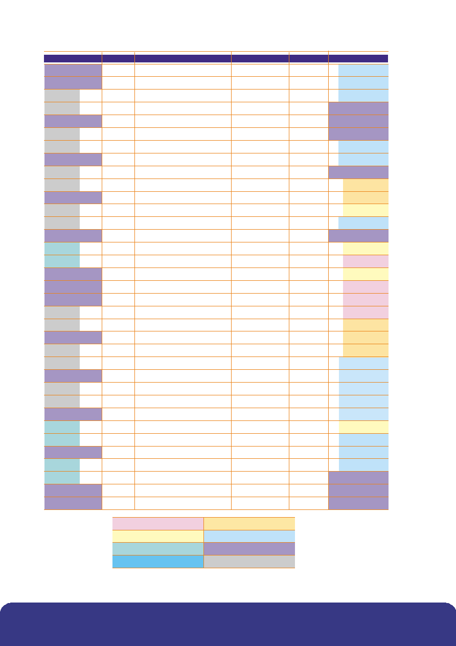
Pin Assignment
Tx and Rx Pin out
www.bookham.com
Thinking optical solutions
www.bookham.com
Thinking optical solutions


