Data
sheet
www.bookham.com
Thinking RF solutions
GaAs MMIC for
2.4GHz Wireless
Lan Applications
The P35-4712-1 is a high performance Gallium Arsenide
Monolithic Microwave Integrated Circuit (GaAs MMIC)
transceiver for wireless LAN applications in the 2.4GHz ISM
band. It is designed for use with the P35-4775-1. Power
amplifier and T/R switch, for transceivers requiring >=20dBm
output power. Low receive current requirements make it
particularly useful for battery powered operation.
Features
∑ Extremely low standby current
for whole chip (<0.5mA)
∑ On chip VCO
∑ Balanced IF input/output
∑ Differential LO is provided for
PLL drive
∑ Low LO leakage
∑ No external biasing, or
matching components required
www.bookham.com
www.bookham.com
Thinking RF solutions
www.bookham.com
Outline Specification
P35-4712-1
Parameter Conditions
Parameters Conditions
RF Frequency
2.4 to 2.5GHz
LO Frequency
2.05 to 2.15 (voltage tuned)
Switching Voltages
0V/-5V (<1mA)
Supply Voltages
+5V
-5V (<1mA)
Receive
Noise figure (SSB)
6dB Typical 7.5dB max
Receive current
38mA Typical
Conversion Gain
9.5dB Typical
7.5dB Minimum
Transmit
Output Power
+6dBm typical
+4dBm minimum
Requires an IF drive of ≠10dBm from 600
differential source
LO leakage
<-20dBm
(without external filtering)
Transmit current
90mA, typical, 125mA max.
IF input impedance
>600
differential
}Into 800
differential load
Low current CMOS interface circuit (M198)
P35-4712-1 Pin Connections
(Pins labelled counter-clockwise from pin 1 which is marked by a dot).
Pin FUNCTION
NOTE
Pin FUNCTION NOTE
1
GND
17
RX
Receive circuits and routing
control, 0V on, -5V off
2
Manufacturers
Leave unconnected
18
IF OUT
Differential IF Outputs
Test Point
(receive)
3
GND
19
IF OUT
Differential IF Outputs
(receive)
4 GND
20 GND
5
Receive Input
LNA input
21
PLL OUT
Differential Oscillator outputs
for PLL
6
N/C
Leave Unconnected
22
PLL OUT
Differential Oscillator outputs
for PLL
7
N/C
Leave Unconnected
23
IF IN
Differential IF Inputs
(transmit)
8
Pre Amp Ramp
Connection for capacitor to
24
IF IN
Differential IF Inputs
slow down pre amp turn on
(transmit)
9
Vdd
+5V supply
25
Pre Amp Enable
Tx amplifiers control,
0V on, -5V off
10
Vdd
+5V supply
26
VCO Enable
VCO and buffer amp control,
0V on, -5V off
11
GND
27
VCO GND
Separate ground for VCO
12
GND
28
VCO Vdd
Separate +5V supply to VCO
13
Pre Amp Out
RF output from up-convertor
29
V tune
LO frequency tuning voltage
14
Vgg
-5V supply
30
Digital GND
Ground point for control
circuit
15
Tx
Transmit routing control, 0V
31
Manufacturers
Leave unconnected
on, -5V off
test point
16 GND
32 GND
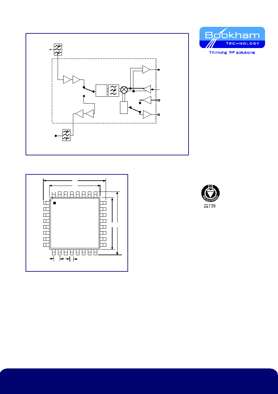
Circuit Diagram for the P35-4712-1
TQFP-32 Plastic Package Outline
Ordering Information
P35-4712-1
LNA
Pre Amp
Diplexer Filter
0
∞
-180
∞
IF Amps
Buffer Amp
0
∞
-180
∞
Balanced
IF Output
Balanced
IF Input
LO
Input
Balanced
PLL Drive
Filter 1
Input
To PA
(P35-4775-1)
Circuit Diagram for the P35-4713 - 1
www.bookham.com
463/SM/00087/000 Issue 1/1
© Bookham Technology 2003 Bookham is a registered trademark of Bookham Technology plc
MMICS
Bookham Technology plc
Caswell
Towcester
Northamptonshire
NN12 8EQ
UK
∑ Tel: +44 (0) 1327 356 789
∑ Fax: +44 (0) 1327 356 698
rfsales@bookham.com
Important Notice
Bookham Technology has a policy of
continuous improvement. As a result
certain parameters detailed on this flyer
may be subject to change without notice.
If you are interested in a particular product
please request the product specification
sheet, available from any RF sales
representative.
P35-4712-1
7.0 9.0
7.0
9.0
32
Pin No. 1
0.8
0.38
9.0
7.0
32
9.0
7.0
0.38
0.8
Pin No. 1