Data
sheet
www.bookham.com
Thinking RF solutions
GaAs MMIC Power
Amplifier ≠ T/R Switch for
1.7 ≠ 2.7GHz Wireless
Applications
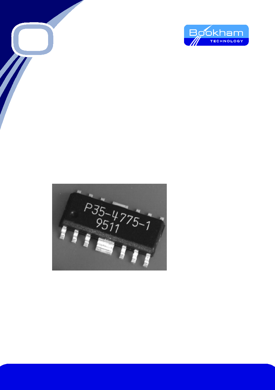
The P35-4775-1 GaAs MMIC contains a two stage power
amplifier, 10dB step attenuator and Tx/Rx switch. This
device is designed to complement the P35-4712 wireless
LAN transceiver MMIC in applications requiring transmit
powers up to 20dBm.
Features
∑ No external biasing or matching
components required
∑ 22dBm Output Power
∑ PCMCIA compatible surface
mount plastic package
∑ 10dB power level step with no
degradation in intermodulation
performance
www.bookham.com

www.bookham.com
Thinking RF solutions
www.bookham.com
Parameters
Conditions Min
Typ
Max
Units
Gain (dB)
-
20
-
dB
Gain flatness with frequency
-
±1.5
-
dB
Gain variation over temperature
-20∞C to +70∞C
-
±1.0
-
dB
Return losses
-
10
-
dB
Noise figure
-
4.5
-
dB
Saturated output power
Vdd = +5V
-
22
-
dBm
1dB Compression point (P-1dB)
Vdd = +5V
-
18
-
dBm
(High power setting)
Vdd = +7V
-
20
-
dBm
Variation of P-1dB over temp.
-20∞C to +70∞C
-
-
-
dB
Supply currents
Vdd s
-
140
-
mA
Vgg s
-
1
-
mA
Level control
-
10
-
dB
Rx switch loss
-
1.0
-
dB
Electrical Performance
All characteristics applicable over the frequency range 1.7 to 2.7GHz. RF ports are referenced to a characteristic
impedance of 50
. Vdd bias is +5V and Vgg is ≠5V, unless otherwise stated.
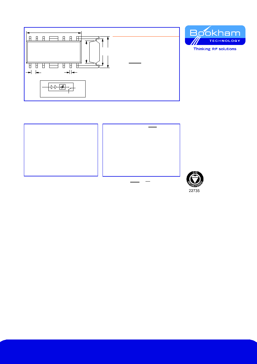
Typical Chip Performance @ 2.4GHz (25∞C)
Functional Block Diagram
Typical Chip Performance @ 2.4GHz (25∞C)
Start .5000 GHz
Stop 5.5000 GHz
CH2 S
21
Log MAG
5dB/
1: 20.368 dB
2.4004 GHz
1
0dB
Tx/Rx
(Antenna)
Rx
RFout
Tx
RFin
Start .5000 GHz
Stop 5.5000 GHz
CH1 S
11
Log MAG
5dB/
1: -11.65 dB
2.4004 GHz
0dB
1
1
0dB
CH1 S
22
Log MAG
5dB/
1: -13.562dB
2.4004 GHz
Start .5000 GHz
Stop 5.5000 GHz
CH2 S
21
Log MAG
5dB/
1: -1.0086 dB
2.4004 GHz
1
0dB
Start .5000 GHz
Stop 5.5000 GHz
CH2 S
21
Log MAG
5dB/
1: -1.0086 dB
2.4004 GHz
1
0dB
Start .5000 GHz
Stop 5.5000 GHz
CH1 S
11
Log MAG
5dB/
1: -11.541 dB
2.4004 GHz
0dB
1
1
0dB
CH1 S
22
Log MAG
5dB/
1: -13.788 dB
2.4004 GHz
P35-4775-1
Absolute Maximum Ratungs
Truth Table
Ordering Information
P35-4775-1
Pin Function
Pin
Function
1 Vgg
8
P
level
2 GND
9
Rx
out
3 PA
Enable
10
Rx
4 GND
11
GND
5 P
level
12
Vdd
6 Tx
13
GND
7 T/R
common
14
PA
in
www.bookham.com
463/SM/00080/000 Issue 2
© Bookham Technology 2003 Bookham is a registered trademark of Bookham Technology plc
10.1 max. (0.396)
14 13 12 11 10 9
8
1 2 3 4 5 6
7
0.4 (0.016)
Dimensions in mm (inches)
4.0 max. (0.157)
5.2 max.
(0.205)
6.2 max.
(0.244)
1.27 (0.05)
Tx/Rx
(Antenna)
Rx
RFout
Tx
RFin
P35-4775-1
MMICS
Bookham Technology plc
Caswell
Towcester
Northamptonshire
NN12 8EQ
UK
∑ Tel: +44 (0) 1327 356 789
∑ Fax: +44 (0) 1327 356 698
rfsales@bookham.com
Important Notice
Bookham Technology has a policy of
continuous improvement. As a result
certain parameters detailed on this flyer
may be subject to change without notice.
If you are interested in a particular product
please request the product specification
sheet, available from any RF sales
representative.
1. N.B. If power level control is not required, P level can
be linked to Tx and P level to RX.
Storage Temperature
-65∞C to 150∞C
Operating Ambient Temp.
-20∞C to =70∞C
Maximum RF Input
+20dBm
Maximum Vdd
+8V
Maximum Vgg
-6V
Soldering Temperature
+250∞C for 5 sec
Channel Temperature
+150∞C
PA enable
Tx
Rx P level P level
Mode of
operation
0V
0V
-5V
0V -5V
Transmit,
High Power
0V
0V
-5V
-5V 0V
Transmit,
Low Power
-5V
-5V
0V
-5V 0V
Receive
-5V
X
-5V
X
X
Standby