Data
sheet
www.bookham.com
Thinking RF solutions
HEMT MMIC
Low Noise Amplifier,
2 - 20GHz
The P35-5104-000-200 and P35-5104-000-301 are a
high performance low noise 2 - 20GHz Gallium Arsenide
monolithic travelling wave amplifiers. They are suitable for
use in broadband communications, instrumentation and
electronic warfare applications. The amplifiers require a
supply of +3.5V and a first gate bias set to give 50% Idss.
Gain is controlled by setting the second gain bias between
the limits of -1V and +1V. An on chip diode is provided for
temperature monitoring for automatic gain control.
The die is fabricated using Bookham's pHEMT process and
is fully protected using Silicon Nitride passivation for
excellent performance and reliability.
Features
∑ Cascode Configuration
∑ 10 dB Gain Typical (-200)
10 dB Min
(-301)
∑ pHEMT technology
∑ AGC control with gate bias
∑ Less than 4.0 dB noise figure
2 - 18GHz
www.bookham.com

www.bookham.com
Thinking RF solutions
www.bookham.com
Parameter Conditions
Min
Typ
Max
Units
Small signal gain (-200)
2GHz - 20GHz
8
10
-
dB
Small signal gain (-301)
2GHz - 20GHz
10
-
-
dB
Ripple on Gain slope
2GHz - 20GHz
-
0.6
±0.6
dB
Gain slope
2
2GHz - 20GHz
-
+1
+1.5
dB
Input Return Loss
2GHz - 20GHz
9
12
-
dB
Output Return Loss
2GHz - 20GHz
9
15
-
dB
Output power at 1dB
10GHz
10
13
-
dBm
gain compression
18GHz `
7
8
-
dBm
Noise figure
1
2GHz - 18GHz
-
-
4.0
dB
18GHz - 20GHz
-
-
4.5
dB
IP3 10GHz
-
22
-
dBm
18GHz -
19
-
dBm
2nd Harmonic
Input Freq. = 9GHz
-
-25dBc
-
dBc
Input Power = -18dBm
Bias supply current (Idd)
-
70
110
mA
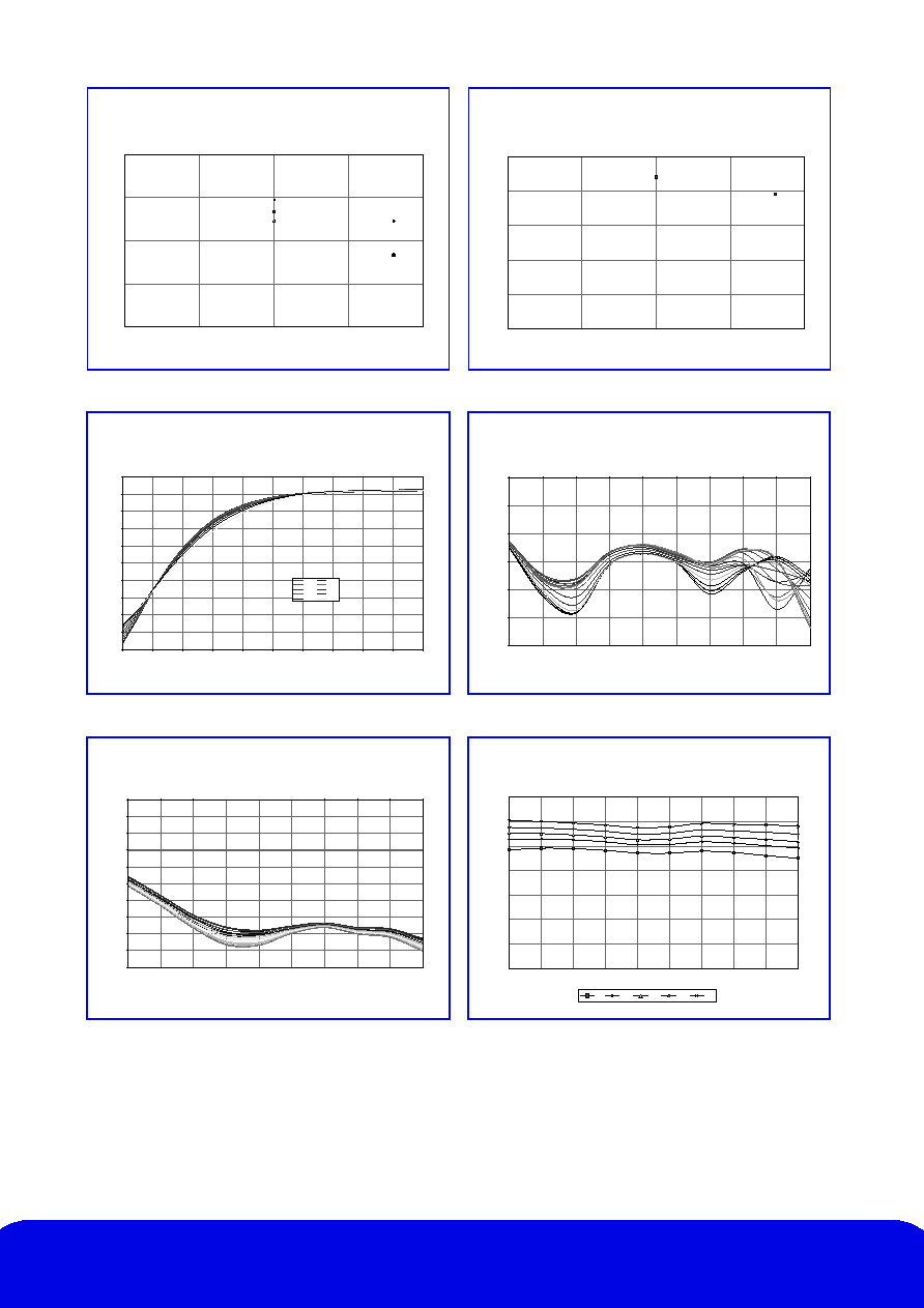
Electrical Performance
Ambient temperature = 22±3∞ C, Zo = 50
, Vdd = 3.5V, Vg1 set for Idd = 0.5 Idss, Vg2 = +1.0V
0
2
4
6
8
10
12
14
0
2
4
6
8
10
12
14
16
18
20
Frequency (GHz)
Gain (dB)
22∞C
-40∞C
85∞C
0
1
2
3
4
5
6
0
2
4
6
8
10
12
14
16
18
20
Frequency (GHz)
Noise Figure (dB)
0
5
10
15
20
25
30
35
40
45
2
4
6
8
10
12
14
16
18
20
Frequency (GHz)
Return Loss (dB)
0
5
10
15
20
25
2
4
6
8
10
12
14
16
18
20
Frequency (GHz)
Return Loss (dB)
P35-5104-000-200
Gain
Noise Figure
Input Return Loss (dB)
Output Return Loss (dB)
Notes
1. Noise Figure assumes inclusion of bond wire inductance at input
2. Least Squares Linear fit.
Typical RFOW Performance
Thinking RF solutions
www.bookham.com
0
5
10
15
20
0
5
10
15
20
Frequency (GHz)
Output Power (dBm)
0
5
10
15
20
25
0
5
10
15
20
Frequency (GHz)
IP3 (dBm)
-35
-30
-25
-20
-15
-10
-5
0
5
10
15
-1
-0
.8
-0
.6
-0
.4
-0
.2
0
0.
2
0.
4
0.
6
0.
8
1
Vg2 (V)
Gain (dB)
2GHz
4GHz
6GHz
8GHz
10GHz
12GHz
14GHz
16GHz
18GHz
20GHz
0
5
10
15
20
25
30
2
4
6
8
10
12
14
16
18
20
Frequency (GHz)
Return Loss (dB)
Output power at 1dB compression
Third Intercept (dBm)
Gain +22∞ C
Vg2 - 1V to +1V step 0.1V
Input Return Loss (dB) +22∞ C
Vg2 - 1V to +1V step 0.1V
0
2
4
6
8
10
12
14
16
18
20
2
4
6
8
10
12
14
16
18
20
Frequency (GHz)
Output Return Loss (dB)
0
2
4
6
8
10
12
14
2
4
6
8
10
12
14
16
18
20
Frequency (GHz)
(dB)
5th
25th
50th
75th
95th
Output Return Loss (dB) +22∞ C
Vg2 - 1V to +1V step 0.1V
Gain (27000 Devices)

Thinking RF solutions
www.bookham.com
-40
-35
-30
-25
-20
-15
-10
-5
0
2
4
6
6
10
12
14
16
18
20
Frequency (GHz)
(dB)
5th
25th
50th
75th
95th
-40
-35
-30
-25
-20
-15
-10
-5
0
2
4
6
8
10
12
14
16
18
20
Frequency (GHz)
(dB)
5th
25th
50th
75th
95th
Output Return Loss (27000 Devices)
Input Return Loss (27000 Devices)
Gain Control
Electrical Schematic
Parameter Conditions
Min
Typ
Max
Units
Gain change at 10GHz
Vg2 = -0.5V
-
-7
-
dB
with respect to Vg2=0V
Vg2 = +1V
-
+2
-
dB
Gate voltage gain control range
Vg2
-1
-
+1
Volts
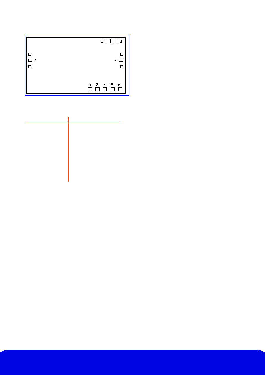
Chip Outline
Pad Details
Die size
3.15 x 1.78mm
Bond pad size
120µm x 80µm
All oyther bond pads 120µm x 120µm
Die thickness:
100µm
Pad Function
1 RF
Input
2 Vdd
3 GND
4
RF Output
5
Vg2 (Gain control)
6 Vg1
7 GND
8 Diode
Vd+
9 Diode
Vd-
Thinking RF solutions
www.bookham.com
Handling and Assembly Information
Gallium Arsenide (GaAs) devices are susceptible to electrostatic and mechanical damage. Dice are supplied in
antistatic containers, which should be opened in cleanroom conditions at an appropriately grounded anti-static
workstation. Devices need careful handling using correctly designed collets, vacuum pickups or, with care, sharp
tweezers.
GaAs Products from Caswell Technology's pHEMT Foundry process are 100 µm thick and have through GaAs
vias to enable grounding to the circuit. Windows in the surface passivation above the bond pads are provided to
allow wire bonding to the die.
The surface to which the die are to be attached should be cleaned with a proprietary de-greasing cleaner.
Conductive epoxy mounting is recommended for the assembly of pHEMT circuits. Recommended epoxies are
Ablestick 84-1LMI or 84-1LMIT cured at 150 ∞C for 1 hour in a nitrogen atmosphere. The epoxy should be applied
sparingly to avoid encroachment of the epoxy on to the top surface of the die. An epoxy fillet should be visible
around the total die periphery.
Eutectic mounting can also be used and entails the use of a gold-tin (AuSn) preform, approximately 0.001" thick,
placed between the die and the attachment surface. The preferred method of mounting is the use of a machine
such as a Mullins 8-140 die bonder. This utilises a heated collet and workstation with a facility for applying a
scrubbing action to ensure total wetting and avoid the formation of voids. Dry nitrogen gas is directed across the
work piece.
The gold-tin eutectic (80% Au 20% Sn) has a melting point of approximately 280 ∞C(Note: Gold Germanium with
a higher melting temperature should be avoided, in particular for MMICs). The work station temperature should be
310 ∞C ± 10 ∞C. The collet should be heated, and the die pre-heated to avoid excessive thermal shock. The
strength of the bonding formed by this method will result in fracture of the die, rather than the bond under die
strength testing.