Data
sheet
www.bookham.com
Thinking RF solutions
HEMT MMIC LNA
8.5 ≠ 10.5GHz
The P35-5112-000-200 is an 8.5 ≠ 10.5GHz Gallium
Arsenide low noise amplifier. This product is intended for
use in a wide range of applications including
telecommunications, instrumentation and electronic warfare.
The die is fabricated using Bookham Technology's 0.20µm
gate length, pHEMT process and is fully protected using
Silicon Nitride passivation for excellent performance and
reliability.
Features
∑ 19dB Gain Typical
∑ 1dB Noise Figure
www.bookham.com
www.bookham.com
Thinking RF solutions
www.bookham.com
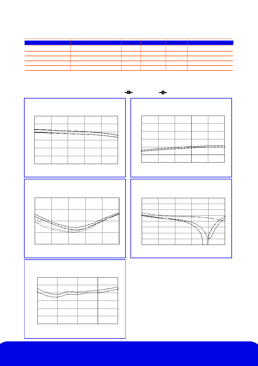
Parameter Conditions
Min
Typ
Max
Units
Small Signal Gain
8.5-10.5GHz
-
18
-
dB
Input Return Loss
8.5-10.5GHz
-
10
-
dB
Output Return Loss
8.5-10.5GHz
-
16
-
dB
Noise Figure
8.5-10.5GHz
-
1.0
-
dB
Supply current,
Idd By Adjustment of Vg1/Vg2
-
32
-
mA
Electrical Performance
Ambient Temperature = 22±3∞ C, Zo = 50
, Vd = 2V, Vg1 set for Id1=12mA, Vg2 set for Id2 = 20mA
0
5
10
15
20
25
30
35
40
10
11
12
7
8
9
Frequency (GHz)
Return Loss (dB)
P35-5112-000-200
Output Return Loss (dB)
Notes
1. All parameters measured on wafer
Typical RFOW Performance ( ----- With Bondwires ) (Id1,Id2) (20mA, 35mA) (12mA, 20mA)
0
5
10
15
20
10
11
12
7
8
9
Frequency (GHz)
Return Loss (dB)
0
5
10
15
20
25
30
10
7
8
9
11
12
Frequency (GHz)
Gain (dB)
0
0.25
0.5
0.75
1
1.25
1.5
7
8
9
10
11
Frequency (GHz)
Noise Figure (dB)
Gain
0
10
20
30
40
50
60
9
7
8
10
11
12
Frequency (GHz)
Isolation (dB)
Reverse
Noise Figure
Input Return Loss (dB)

Thinking RF solutions
www.bookham.com
Handling and Assembly Information
Gallium Arsenide (GaAs) devices are susceptible to electrostatic and mechanical damage. Dice are supplied in
antistatic containers, which should be opened in cleanroom conditions at an appropriately grounded anti-static
workstation. Devices need careful handling using correctly designed collets, vacuum pickups or, with care, sharp
tweezers.
GaAs Products from Bookham Technology's pHEMT Foundry process are 100µm thick and have through GaAs
vias to enable grounding to the circuit. Windows in the surface passivation above the bond pads are provided to
allow wire bonding to the die.
The surface to which the die are to be attached should be cleaned with a proprietary de-greasing cleaner.
Conductive epoxy mounting is recommended. Recommended epoxies are Ablestick 84-1LMI or 84-1LMIT cured
at 150∞C for 1 hour in a nitrogen atmosphere. The epoxy should be applied sparingly to avoid encroachment of
the epoxy on to the top surface of the die. An epoxy fillet should be visible around the total die periphery.
Eutectic mounting should be used and entails the use of a gold-tin (AuSn) preform, approximately 0.001∞¬ thick,
placed between the die and the attachment surface. The preferred method of mounting is the use of a machine
such as a Mullins 8-140 die bonder. This utilises a heated collet and workstation with a facility for applying a
scrubbing action to ensure total wetting and avoid the formation of voids. Dry nitrogen gas is directed across the
work piece.
The gold-tin eutectic (80% Au 20% Sn) has a melting point of approximately 280∞C (Note: Gold Germanium with
a higher melting temperature should be avoided, in particular for MMICs). The work station temperature should be
310∞C ± 10∞C. The collet should be heated, and the die pre-heated to avoid excessive thermal shock. The
strength of the bonding formed by this method will result in fracture of the die, rather than the bond under die
strength testing.
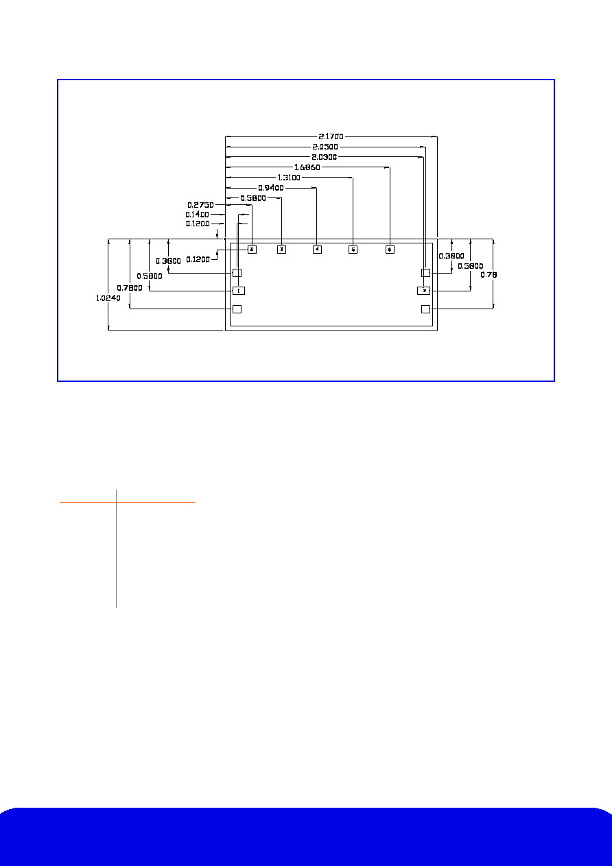
The P35-5112-000-200 amplifier die has gold bond pads. The recommended wire bonding procedure uses 25µm
(0.001") 99.99% pure gold wire with 0.5-2% elongation. Thermo-compression wedge bonding is preferred though
thermosonic wire bonding may be used providing the ultrasonic content of the bond is minimised. A work station
temperature of 260∞C ± 10∞C with a wedge tip temperature of 120∞C ± 10∞C is recommended. The wedge force
should be 45 ± 5 grams. Bonds should be made from the bond pads on the die to the package or substrate.
The RF bond pads at the input and output are 120µm x 80µm; all other bond pads are 120µm x 120µm.
The P35-5112-000-200 has been designed to include the inductance of a single 25µm bond wire at both the input
and output, facilitating the integration of the die into a 50
environment, these should be kept to a minimum
length.
Operating and Biasing of the P35-5112-000-200
The P35-5112-000-200 is a two-stage low noise amplifier. The drain biases for both stages (Vd1 & Vd2) are
accessible and should be set to 2 volts. The gate voltages (Vg1 & Vg2) are set to give 12mA of drain current in the
first stage and 20mA in the second stage drain. The separate drain and gate voltage supplies for both stages can
be combined into single supplies (Vdd & Vgg). As with most GaAs devices gate voltages should be applied before
connecting the drain supply. DC bias supplies should be decoupled to ground using 100pF chip capacitors
placed close to the chip with short bondwires to the amplifier bond pads.
P35-5112-000-200
P35-5112-000-200