Data
sheet
www.bookham.com
Thinking RF solutions
HEMT MMIC LNA
20 - 32GHz
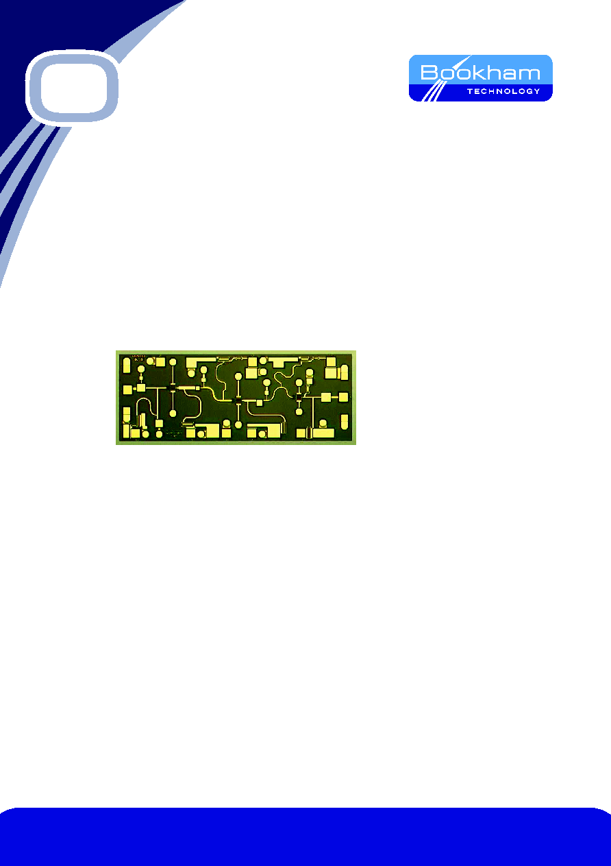
The P35-5114-00-200 is a 20-32GHz Gallium Arsenide low
noise amplifier. This product is intended for use in fixed-
point and point to point microwave systems.
The die is fabricated using Bookham Technology's 0.20µm
gate length, pHEMT process and is fully protected using
Silicon Nitride passivation for excellent performance and
reliability.
Features
∑ Typical 2.2dB Noise Figure
@24GHz to 28GHz
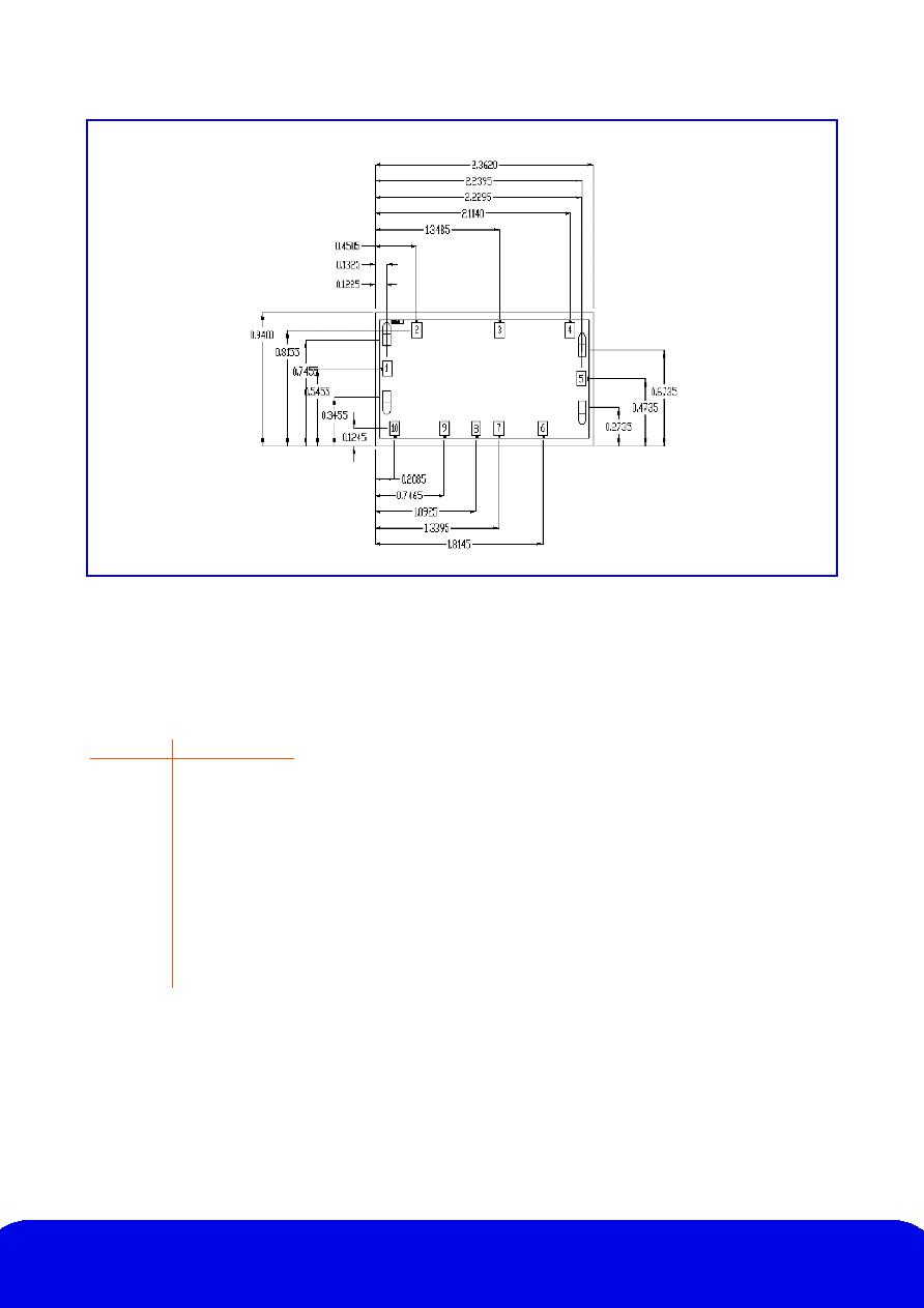
∑ 2.36 x 0.94mm Die Size
www.bookham.com
www.bookham.com
Thinking RF solutions
www.bookham.com
Parameter Conditions
Min
Typ
Max
Units
Small Signal Gain
20-32GHz
18
21
-
dB
Input Return Loss
20-32GHz
6
12
-
dB
Output Return Loss
20-32GHz
6
12
-
dB
Noise Figure
24GHz
-
2.2
3.0
dB
Noise Figure
28GHz
-
2.2
3.0
dB
P1dB
20-32GHz
4
7
-
dBm
Drain current, Id1
-
13
-
mA
Drain current, Id2
-
13
-
mA
Drain current, Id3
-
22
-
mA
Gate Voltage; Vg1
-
-0.6
-
V
Gate Voltage; Vg2
-
-0.6
-
V
Gate Voltage; Vg3
-
-0.4
-
V
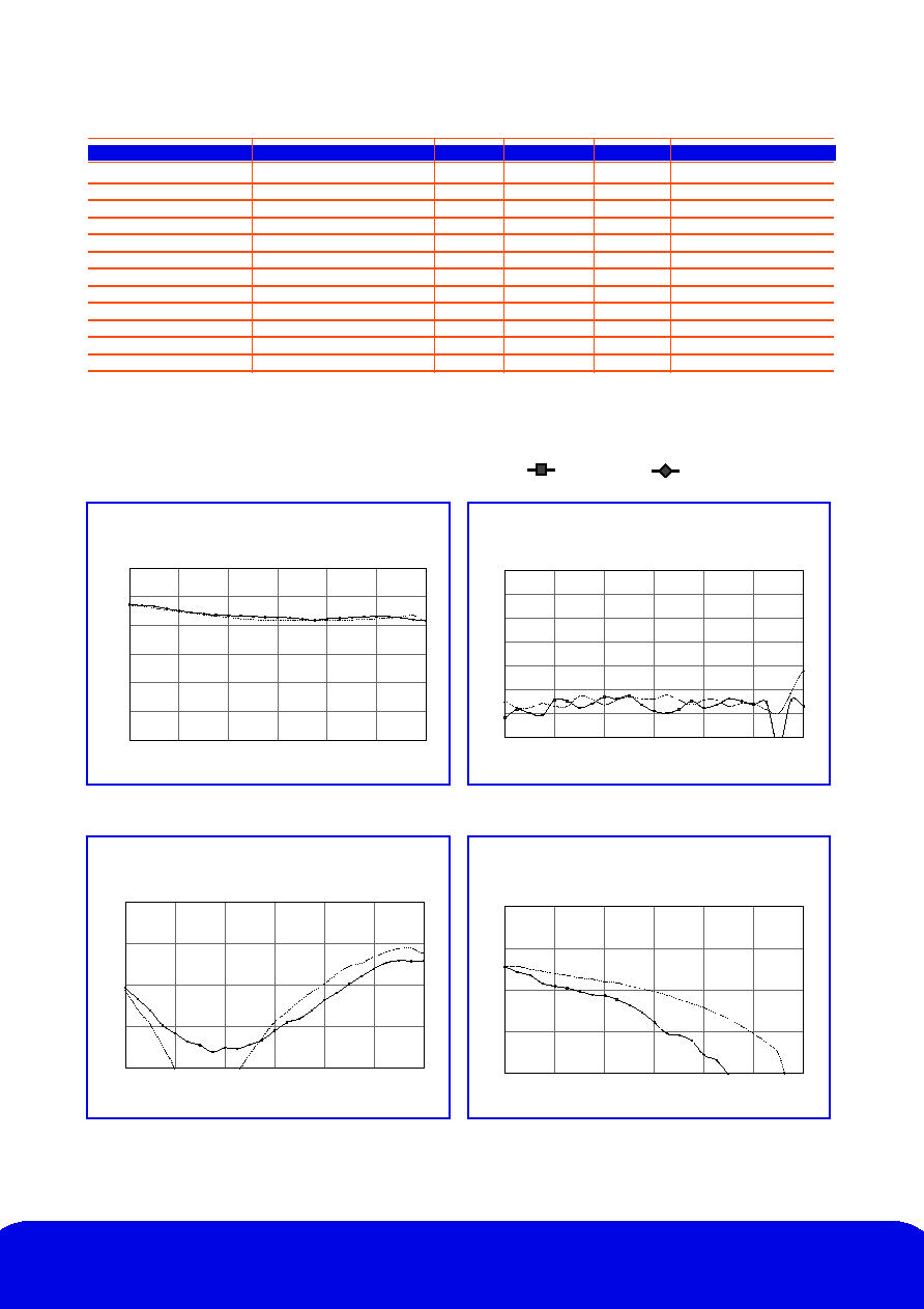
Typical RFOW Performance ( ----- Jig Meas ) (Vd1,Vd2,Vd3) (2V,2V,2V) (2V,2V,3V)
Electrical Performance
Ambient Temperature = 22±3∫ C, Zo = 50
, Vd = 2V, Vg1 & Vg2 set for Id1=Id2=13mA, Vg3 set for Id3=22mA
0
5
10
15
20
20
22
24
26
28
30
32
Frequency (GHz)
Return Loss (dB)
P35-5114-000-200
Output Return Loss (dB)
Notes
1. All parameters measured on wafer
0
5
10
15
20
20
22
24
26
28
30
32
Frequency (GHz)
Return Loss (dB)
0
5
10
15
20
25
30
20
22
24
26
28
30
32
Frequency (GHz)
Gain (dB)
Gain
0
10
20
30
40
50
60
70
20
22
24
26
28
30
32
Frequency (GHz)
Isolation (dB)
Reverse Isolation
Input Return Loss (dB)
Thinking RF solutions
www.bookham.com
P35-5114-000-200
15
17
19
21
23
25
20
22
24
26
28
30
32
Frequency (GHz)
Gain (dB)
-25∞C
25∞C
50∞C
75∞C
Gain (Vdd 2v, Vgg=-0.4V)
1.0
1.5
2.0
2.5
3.0
3.5
4.0
26
27
28
29
30
31
Frequency (GHz)
Noise Figure (dB)
-25∞C
25∞C
50∞C
75∞C
0
1
2
3
4
20
22
24
26
28
30
32
Frequency (GHz)
Noise Figure (dB)
Noise Figure
0
2
4
6
8
10
20
22
24
26
28
30
32
Frequency (GHz)
P1dB (dBm)
P1db
Noise Figure (Vdd 2v, Vgg=-0.4V)
-25
-20
-15
-10
-5
0
20
22
24
26
28
30
32
Frequency (GHz)
Return Loss (dB)
5th
25th
50th
75th
95th
Input Return Loss (2700 devices)
0
5
10
15
20
25
20
22
24
26
28
30
32
Frequency (GHz)
Gain (dB)
5th
25th
50th
75th
95th
Gain (2700 devices)
-40
-35
-30
-25
-20
-15
-10
-5
0
20
22
24
26
28
30
32
Frequency (GHz)
Return Loss (dB)
5th
25th
50th
75th
95th
Output Return Loss (2700 devices)
Typical RFOW Performance