 | –≠–ª–µ–∫—Ç—Ä–æ–Ω–Ω—ã–π –∫–æ–º–ø–æ–Ω–µ–Ω—Ç: 2FAM-C5R | –°–∫–∞—á–∞—Ç—å:  PDF PDF  ZIP ZIP |
2FAM-C5R - Integrated Passive & Active Device using CSP
Specifications are subject to change without notice.
Customers should verify actual device performance in their specific applications.
SOLDER
BUMPS
SILICON
DIE
Electrical Characteristics
Symbol
Minimum
Nominal
Maximum
Unit
(T
A
= 25 ∞C unless otherwise noted)
Per Line Specification
Resistance
R
8
10
12
Capacitance @ 0 V 1 MHz
C
32
40
48
pF
Rated Standoff Voltage
V
WM
5.0
V
Breakdown Voltage @ 1 mA
V
BR
6.0
V
Forward Voltage @ 10 mA
V
F
0.8
V
Leakage Current @ 3.3 V
I
R
0.1
0.5
µA
Filter Attenuation @ 800 - 3000 MHz
S21
-25
-30
dB
ESD Protection: IEC 61000-4-2
Contact Discharge
±8
kV
Air Discharge
±15
kV
Thermal Characteristics
(T
A
= 25 ∞C unless otherwise noted)
Operating Temperature Range
T
J
-40 25 +85 ∞C
Storage Temperature Range
T
STG
-55 25 +150 ∞C
Power Dissipation Per Resistor
P
D
100 mW
General Information
Features
Lead free versions available
RoHS compliant (lead free version)*
Bidirectional EMI filtering
ESD protection
Protects two audio lines
Applications
Cell phones
PDAs and notebooks
Digital cameras
MP3 players and GPS
Electrical & Thermal Characteristics
The 2FAM-C5R device, manufactured using Thin Film on
Silicon technology, provides ESD protection and EMI
filtering for the audio port of portable electronic devices
such as cell phones, modems and PDAs. The device
incorporates two low pass filter channels where each
channel has a series 10 ohm resistor assuring a minimum
of -25 dB attenuation from 800 MHz to 3 GHz. The device
is suitable for EMI filtering of GSM, CDMA, W-CDMA,
WLAN and Bluetooth frequencies.
Each internal and external port of the two channels
includes a TVS diode for ESD protection. The ESD
protection provided by the component enables a data
port to withstand a minimum ±8 KV Contact / ±15 KV Air
Discharge per the ESD test method specified in IEC
61000-4-2. The device measures 1.00 mm x 1.33 mm and
is available in a 5 bump CSP package intended to be
mounted directly onto an FR4 printed circuit board. The
CSP device meets typical thermal cycle and bend test
specifications without the use of an underfill material.
*RoHS COMPLIANT
VERSIONS
AVAILABLE
*RoHS Directive 2002/95/EC Jan 27 2003 including Annex
DIMENSIONS =
MILLIMETERS
(INCHES)
Specifications are subject to change without notice.
Customers should verify actual device performance in their specific applications.
Mechanical Characteristics
2FAM-C5R - Integrated Passive & Active Device using CSP
B2
A1
A3
C3
C1
0.432 - 0.559
(0.017 - 0.022)
0.971 - 1.001
(0.038 - 0.039)
0.330 - 0.457
(0.013 - 0.018)
1.285 - 1.375
(0.051 - 0.054)
0.180 - 0.280
(0.007 - 0.011)
0.435
(0.017)
0.435
(0.017)
0.3
(0.012)
0.180 - 0.280
(0.007 - 0.011)
DIA.
0.50
(0.020)
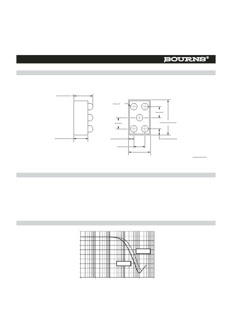
This is a silicon-based device and is packaged using chip scale packaging technology. Solder bumps, formed on the silicon die,
provide the interconnect medium from die to PCB. The bumps are arranged on the die in a regular grid formation. The grid pitch is
0.5 mm and the dimensions for the packaged device are shown below.
Reliability data is gathered on an ongoing basis for Bourns
Æ
Integrated Passive and Active Devices.
"Package level" testing of the integrity of the solder joint is carried out on an independent Daisy-Chain test device. A 25-Pin Daisy
Chain component is available from Bourns for this purpose (part number 2TAD-C25R). This is a 5 x 5 array featuring 0.5 mm pitch
solder bumps. The Distance to Neutral Point (DNP) on that component is larger than that of the 2FAM-C5R and is thus deemed
suitable for Thermal Cycle testing.
"Silicon level" reliability performance is based on similarity to other integrated passive CSP devices from Bourns.
Reliability Data
Frequency Response
Frequency (MHz)
Gain (dB)
0.1
1
10
0 Volts
2.5 Volts
100
1000
10000
0
-5
-10
-15
-20
-25
-30
-35
-40
-45
-50
Specifications are subject to change without notice.
Customers should verify actual device performance in their specific applications.
2FAM-C5R - Integrated Passive & Active Device using CSP
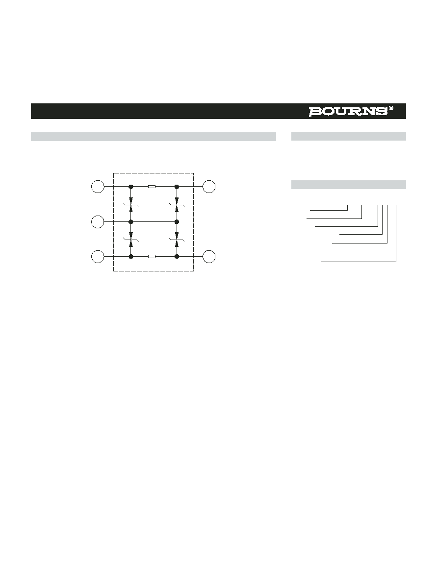
Block Diagram
GND
R1:
10 OHMS
R2:
10 OHMS
EXT1
INT1
EXT2
INT2
The CSP device block diagram below includes the pin names and basic electrical
connections associated with each channel.
Please consult the "Bourns Design
Guide Using CSP" for notes on PCB
design and SMT Processing.
PCB Design and SMT Processing
How to Order
2 FAM - C5R __
__
Thinfilm
Model
Chipscale
No. of Solder Bumps
Packaging Option
R = Tape and Reel
Packaged 3000 pcs. / 7 " reel
Terminations
LF = Sn/Ag/Cu (lead free)
Blank = Sn/Pb
Specifications are subject to change without notice.
Customers should verify actual device performance in their specific applications.
2FAM-C5R - Integrated Passive & Active Device using CSP
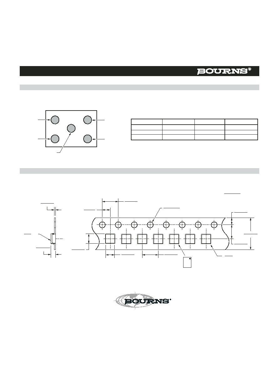
The pin-out for the device is shown below with the bumps facing up.
Device Pin Out
The surface mount product is packaged in an 8 mm x 4 mm Tape and Reel format per EIA-481 standard.
Packaging
1
2
3
GND
EXT2
C
B
A
EXT1
INT2
INT1
2.0 ± 0.05
(.08 ± .002)
0.3 ± 0.05
(.01 ± .002)
1.18 ± 0.1
(.05 ± .004)
1.52 ± 0.1
(.06 ± .004)
1.75 ± 0.1
(.07 ± .004)
3.5 ± 0.05
(.14 ± .002)
8.0 ± 0.3
(.31 ± .01)
0.76 ± 0.1
(.03 ± .004)
ORIENTATION
OF COMPONENT
IN POCKET
BACKSIDE FACING UP
TOP SIDE VIEW
(INTO COMPONENT POCKET)
0.3
(0.01)
4.0 ± 0.1
(.16 ± .004)
4.0 ± 0.1
(.16 ± .004)
0.25
(0.010)
TYP.
R
1.5 ± 0.1/-0
(.06 ± .004/-0)
DIA.
MAX.
R
Pin Out
Function
Pin Out
Function
A1
EXT1
A3
INT1
C1
EXT2
C3
INT2
B2
GND
DIMENSIONS =
MILLIMETERS
(INCHES)
Asia-Pacific:
TEL +886- (0)2 25624117 ∑ FAX +886- (0)2 25624116
Europe:
TEL +41-41 768 5555 ∑ FAX +41-41 768 5510
The Americas: TEL +1-951 781-5492 ∑ FAX +1-951 781-5700
www.bourns.com
Reliable Electronic Solutions
COPYRIGHT© 2004, BOURNS, INC. LITHO IN U.S.A. 08/04 e/IPA0411
2FAM-C5R REV. D, 02/05