*RoHS Directive 2002/95/EC Jan 27 2003 including Annex
Specifications are subject to change without notice.
Customers should verify actual device performance in their specific applications.
R1
R2
R1
R2
R3
R4
CAT16-F4, -J4
CAY16-F4, -J4
R1
R2
R3
R4
CAT16-F8, -J8
CAY16-J8
R5
R6
R7
R8
CAT16-J2
CAY16-J2
CAT/CAY 16 Series - Chip Resistor Arrays
Features
Lead free version available (see How to Order "Termination" options)
Lead free versions are RoHS compliant*
Convex and concave terminals
2, 4 or 8 isolated elements available
Resistance tolerance ±1 % and ±5 %
Resistance range: 10 ohms to 1 megohm
Specifications
Requirement
Characteristics
Test Method
Short Time Overload
±1 % (±2 % for CAT16-F8, -J8 & CAY16-J8)
Rated Voltage X 2.5, 5 seconds
Soldering Heat
±1 %
260 ∞C ±5 ∞C, 10 seconds ±1 second
Temperature Cycling (5)
±1 %
125 ∞C (30 minutes) - normal (15 minutes)
-30 ∞C (30 minutes) - normal (15 minutes)
Moisture Load Life
±2 % (±3 % for CAT16-F8, -J8 & CAY16-J8)
1000 hours
Load Life
±2 % (±3 % for CAT16-F8, -J8 & CAY16-J8)
1000 hours
Characteristics
Schematics
Characteristics
CAT16/CAY16
Number of Elements
2 (J2), 4 (F4, J4), 8 (F8, J8)
Power Rating Per Resistor
62 mW (31 mW for CAY16-J8)
Resistance Tolerance
±1 %, ±5 %
Resistance Range: E24 (J), E96 + E24 (F)
10 ohms - 1 megohm
Zero-Ohm Jumper < 0.05 ohm
Max. Working Voltage
50 V (25 V for CAY16-J8)
Operating Temp. Range
-55 ∞C - 125 ∞C
How To Order
CA Y 16 - 103 J 4 __
Chip Arrays
Type
∑ T = Concave
∑ Y = Convex
Models
∑ J2 = 0606 Package Size
∑ F4, J4 = 1206 Package Size
∑ F8 = 2406 Package Size for CAT16
∑ J8 = 2406 Package Size for CAT16;
1506 Package Size for CAY16
Resistance Code
∑ 103 = 10 K ohms
∑ 1003 = 100 K ohms (1 % tolerance)
∑ 000 = Zero-ohm
Resistance Tolerance
∑ J = ±5 % (Use "J" for zero-ohm jumper)
∑ F = ±1 % (4 resistor package and CAT16-F8)
Resistors
∑ 2 = 2 Isolated Resistors
∑ 4 = 4 Isolated Resistors
∑ 8 = 8 Isolated Resistors
Terminations*
∑ LF = Tin-plated (lead free)
∑ Blank = Solder-plated
*Model CAY16-J8 is available only with tin-plated
terminations.
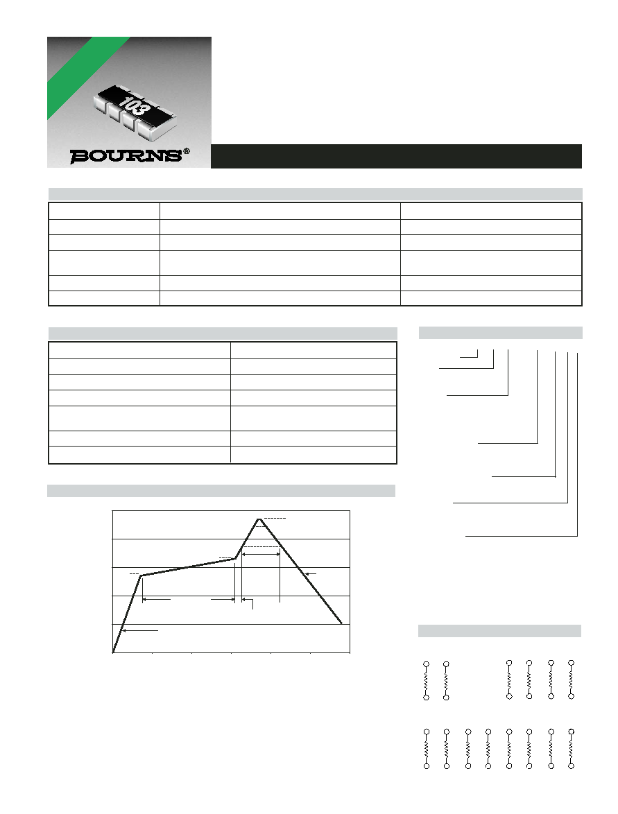
Soldering Profile for Lead Free Chip Resistors and Arrays
25
75
125
175
225
275
0
50
100
150
200
250
300
Time (seconds)
Temperature (∞C)
60 - 120 seconds
60 - 90
seconds
260 ∞C peak
190 ∞C
150 ∞C
220 ∞C
Ramp Down
3 ∞C/second
255 ∞C
Maximum of 20 seconds between
+255 ∞C and +260 ∞C
Ramp Up
3 ∞C/second maximum
10 seconds minimum
<1>
<1>
*RoHS COMPLIANT
VERSIONS
AVAILABLE
For Standard Values Used in Capacitors,
Inductors, and Resistors,
click here.
Specifications are subject to change without notice.
Customers should verify actual device performance in their specific applications.
REV. 07/06
Model
a
b
p
f
CAT16-F4, -J4, -F8, -J8
0.7 to 0.9
0.4 to 0.45
0.80
2.0 to 2.2
(.028 to .035)
(.016 to .0178)
(.032)
(.079 to .087)
CAY16-F4, -J4
0.7 to 0.9
0.4 to 0.45
0.80
2.4 to 2.8
(.028 to .035)
(.016 to .0178)
(.032)
(.094 to .11)
CAY16-J8
0.7 to 0.9
0.3 to 0.35
0.50
2.0 to 2.2
(.028 to .035)
(.012 to .014)
(.020)
(.079 to .087)
CAT16-J2
0.7 to 0.9
0.4 to 0.45
0.80
2.2 to 2.6
(.028 to .035)
(.016 to .0178)
(.032)
(.087 to .102)
CAY16-J2
0.7 to 0.9
0.4 to 0.5
0.80
2.0 to 2.6
(.028 to .035)
(.016 to .020)
(.032)
(.079 to .102)
DIMENSIONS ARE:
MM
(INCHES)
CAT/CAY 16 Series - Chip Resistor Arrays
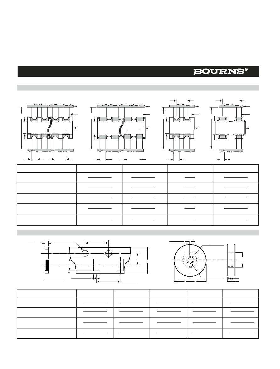
Land Patterns
Packaging Dimensions
Model
a
b
c
d
e
CAT16-F4, -J4 & CAY16-F4, J4
3.40 ± 0.10
3.50 ± .005
8.0 ± 0.3
9.0 ± 0.3
11.4 ± 1.0
(.134 ± .004)
(.138 ± .004)
(.315 ± .012)
(.354 ± .012)
(.449 ± .040)
CAT16-J2 & CAY16-J2
1.80 ± 0.10
3.50 ± .005
8.0 ± 0.3
9.0 ± 0.3
11.4 ± 1.0
(.070 ± .004)
(.138 ± .004)
(.315 ± .012)
(.354 ± .012)
(.449 ± .040)
CAT16-F8, -J8
6.90 ± 0.20
5.50 ± 0.10
12.0 ± 0.2
13.0 ± 0.2
15.4 ± 1.0
(.272 ± .008)
(.217 ± .004)
(.472 ± .008)
(.512 ± .008)
(.606 ± .040)
CAY16-J8
4.10 ± 0.15
3.50 ± 0.05
8.0 ± 0.3
9.0 ± 0.3
11.4 ± 1.0
(.161 ± .012)
(.138 ± .002)
(.315 ± .012)
(.354 ± .012)
(.449 ± .040)
a
f
b
p
Solder
resist
Land
Chip
resistor
array
a
f
b
p
Solder
resist
Land
Chip
resistor
array
a
f
b
Solder
resist
Land
Chip
resistor
array
p
a
f
b
p
Solder
resist
Land
Chip
resistor
array
CAT16-F4, -J4, -F8, -J8
CAY16-F4, -J4, -J8
CAT16-J2
CAY16-J2
4.0 ± 0.1
(.158 ± .004)
2.0 + 0.1/-0.2
(.08 + .004/-.008)
4.0 ± 0.1
(.157 ± .004)
1.0
(.039)
MAX.
a
c
b
1.5 + 0.1 - 0
(.059 + .004 - 0)
180
(7.087)
2.0 ± 0.5
(.079 ± .020)
60
(2.362)
21.0 ± 0.8
(.827 ± .031)
13.0 ± 0.5
(.511 ± .020)
d
e
∑ 5,000 pcs. per reel (J2, J4, CAY16-J8)
4,000 pcs. per reel (CAT16-F8, -J8)
∑ Paper tape

Specifications are subject to change without notice.
Customers should verify actual device performance in their specific applications.
Cleaning
A recommended cleaning method is shown in the following table.
Component Placement
a. Reduce the mechanical stress to a minimum during and after placing of the unit in order not to damage the terminals and
protective coating.
b. Misplacement of components may cause solder bridges.
Soldering
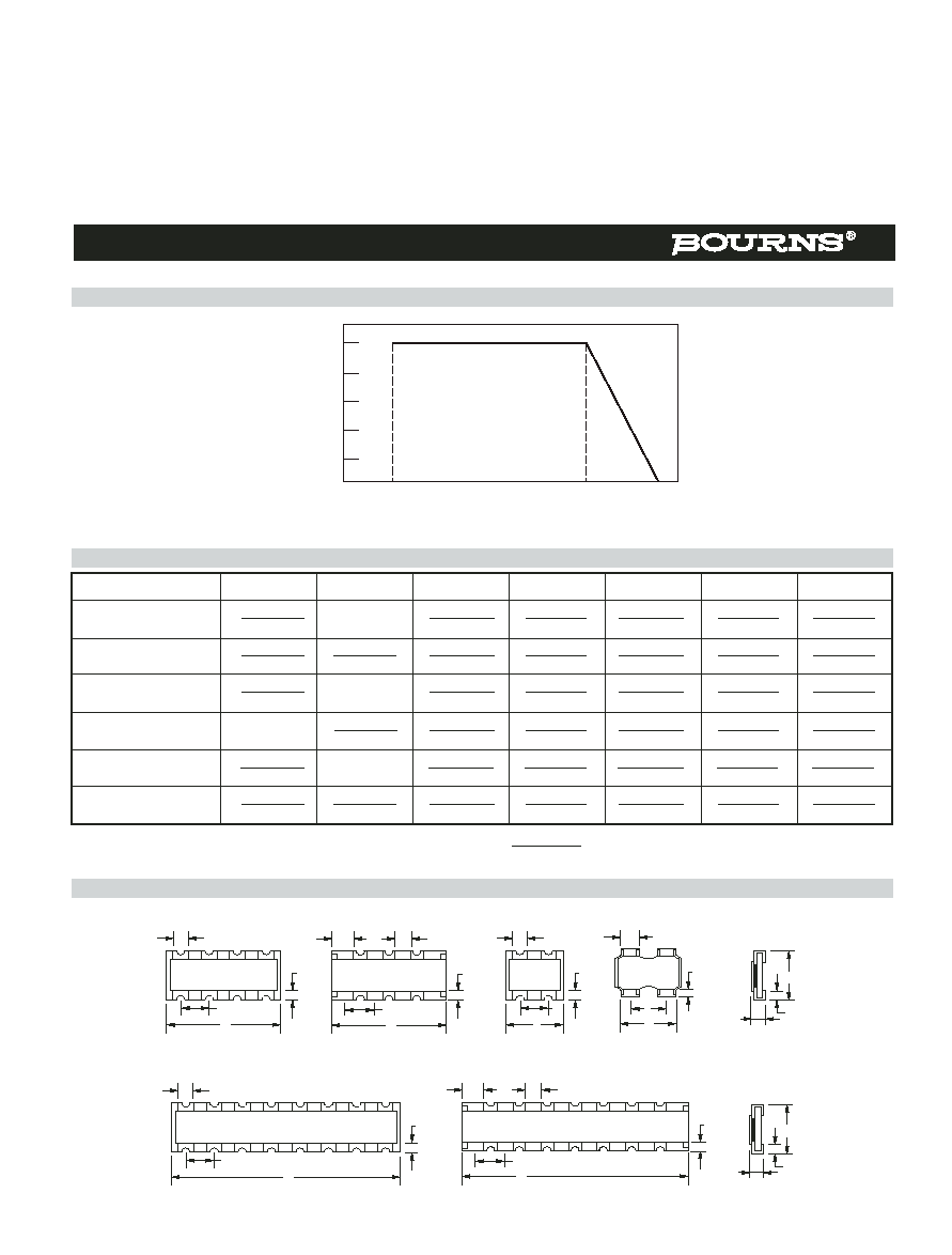
a. Reflow soldering: Recommendation is shown in the following chart.
b. Wave soldering: Recommendation according to IEC standards.
c. Hand soldering: Don't touch the protective coating of the part. Solder within 3 seconds when the temperature is over 280 ∫C.
Cleaning Condition
Solvents
Dipping
Ultrasonic Wave Washing
1 minute maximum
Isopropyl alcohol
5 minutes maximum
Power: 20 W/L
Frequency: 10 to 100 kHz
250
200
150
100
50
0
Preheating
Soldering
Gradual Cooling
60 sec. min.
10-30 sec.
120 sec. min.
T
emperature (°C)
Chip Resistor Arrays - Application Note