*RoHS Directive 2002/95/EC Jan 27 2003 including Annex
Specifications are subject to change without notice.
Customers should verify actual device performance in their specific applications.
Model CAY17 - Bussed Resistor Array
Features
JA version available to 100K ohms
10 pin with 8 resistors in bussed type for
pull up/down circuit
Lead free version available (see How to
Order "Termination" options)
RoHS compliant*
Convex termination style
Resistance tolerance ±5 %
E24 Series from 10 ohms to 43K ohms
Suitable for all types of soldering processes
Paper tape on plastic reel for automatic
placement
Construction
How To Order
CA Y 17 - 103 J A __
Chip Arrays
Type
∑ Y = Convex
Model
∑ 17 = 1206 Package Size
Resistance Code
∑ 103 = 10K ohms
(JA range: 10 ohms to 100K ohms;
JB range: 10 ohms to 43K ohms)
Resistance Tolerance
∑ J = ±5 %
Resistors
∑ A = Common from terminal 5 to 10
∑ B = Common from terminal 1 to 6
Terminations
∑ LF = Tin-plated (lead free)
∑ Blank = Solder-plated
Characteristics
Number of Resistors ....8 (bussed circuit)
Power Rating per Resistor @ 70 ∞C
...................................................31 mW
Package Power Rating @ 70 ∞C
.................................................250 mW
Operating Temperature Range
..................................-55 ∞C to +125 ∞C
Derated to 0 Load @ ..................+125 ∞C
Max. Working Voltage ......................25 V
Max. Overload Voltage.....................50 V
Resistance Tolerance .....................±5 %
Resistance Range/E24 Series
JA version ........10 ohms to 100K ohms
JB version ..........10 ohms to 43K ohms
T.C.R..................................±250 ppm/∞C
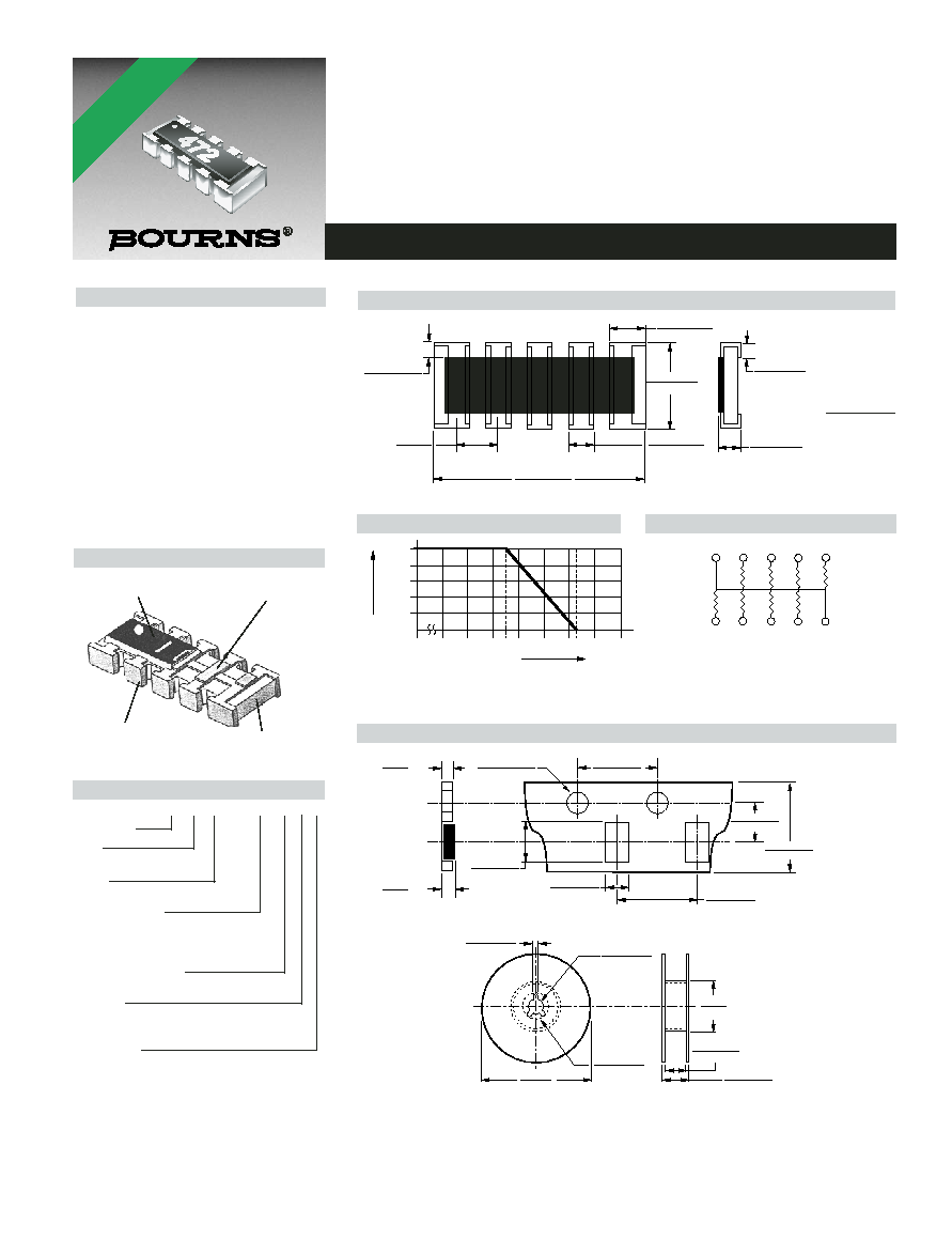
Product Dimensions
1 0 3
1.6 ± 0.2
(.063 ± .008)
0.2 ± 0.15
(.008 ± .006)
0.5 ± 0.1
(.020 ± .004)
0.3 ± 0.2
(.012 ± .008)
0.64
(.025)
3.2 ± 0.2
(.126 ± .008)
0.34 ± 0.15
(.013 ± .006)
0.55 ± 0.1
(.022 ± .004)
Derating Curve
Packaging Dimensions
Protective Glass Overcoat
Thick Film
Resistive Element
Termination
High Purity Alumina
Substrate
4.0 ± 0.1
(.158 ± .004)
3.6 ± 0.2
(.142 ± .008)
2.0 ± 0.2
(.079 ± .008)
4.0 ± 0.1
(.157 ± .004)
1.4
(.055)
MAX.
1.0
(.039)
MAX.
8.0 ± 0.2
(.315 ± .008)
3.5 ± 0.05
(.138 ± .002)
1.5 + 0.1 - 0
(.059 + .004 - 0)
DIMENSIONS:
MM
(INCHES)
Bussed Circuits - Option A
3
4
1
2
10
9
8
7
R
5
6
R
R
R
R
R
R
R
180
(7.087)
2.0 ± 0.5
(.079 ± .020)
60
(2.362)
21.0 ± 0.8
(.827 ± .031)
13.0 ± 0.2
(.511 ± .008)
11.4 ± 1.0
(.449 ± .040)
9.0 ± 0.3
(.354 ± .012)
Rated Load (%)
Ambient Temp. (∞C)
70 ∞C 125
∞C
-55
0
20
40
60
80
100
40
60
80
100 120 140
160
*RoHS COMPLIANT
VERSIONS
AVAILABLE
For Standard Values Used in Capacitors,
Inductors, and Resistors,
click here
.

Specifications are subject to change without notice.
Customers should verify actual device performance in their specific applications.
Model CAY17 - Bussed Resistor Array
REV. 04/06
Soldering Profile for Lead Free Chip Resistors and Arrays
25
75
125
175
225
275
0
50
100
150
200
250
300
Time (seconds)
Temperature (∞C)
60 - 120 seconds
60 - 90
seconds
260 ∞C peak
190 ∞C
150 ∞C
220 ∞C
Ramp Down
3 ∞C/second
255 ∞C
Maximum of 20 seconds between
+255 ∞C and +260 ∞C
Ramp Up
3 ∞C/second maximum
10 seconds minimum
<1>
<1>