*RoHS Directive 2002/95/EC Jan 27 2003 including Annex
MARCH 1994 - REVISED MARCH 2006
Specifications are subject to change without notice.
Customers should verify actual device performance in their specific applications.
TISP3xxxF3 (HV) Overvoltage Protector Series
TISP3240F3, TISP3260F3,
TISP3290F3,TISP3320F3,TISP3380F3
HIGH-VOLTAGE DUAL BIDIRECTIONAL THYRISTOR
OVERVOLTAGE PROTECTORS
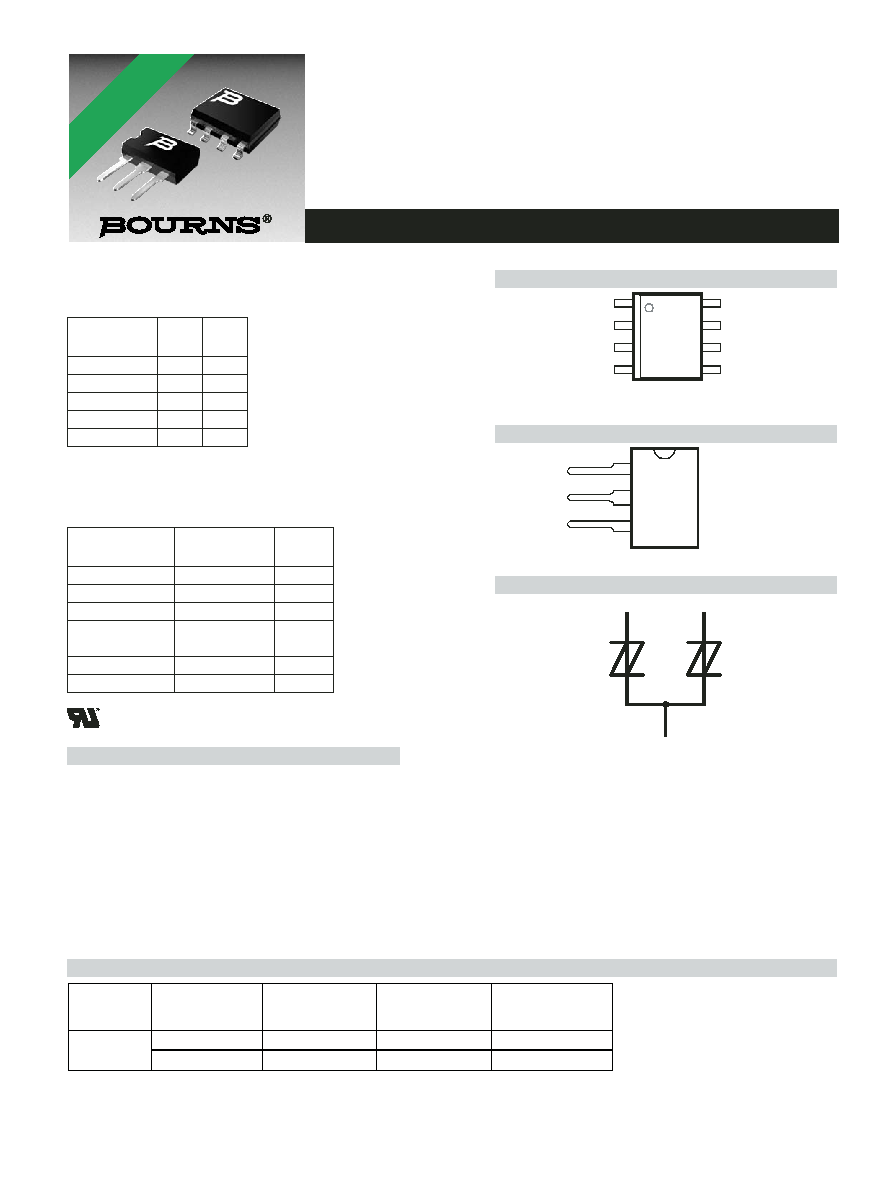
D Package (Top View)
Description
These high-voltage dual bidirectional thyristor protectors
are designed to protect ground backed ringing central
office, access and customer premise equipment against
overvoltages caused by lightning and a.c. power
disturbances. Offered in five voltage variants to meet
battery and protection requirements, they are guaranteed
to suppress and withstand the listed international lightning
surges in both polarities. Overvoltages are initially clipped
by breakdown clamping until the voltage rises to the
breakover level, which causes the device to switch. The
high crowbar holding current prevents d.c. latchup as the
current subsides.
How To Order
Ion-Implanted Breakdown Region
Precise and Stable Voltage
Low Voltage Overshoot under Surge
Planar Passivated Junctions
Low Off-State Current <10 µA
Rated for International Surge Wave Shapes
1
2
3
4
5
6
7
8
G
G
G
G
NC
T
R
NC
NC - No internal connection
SL Package (Top View)
Device Symbol
MD1XAB
1
2
3
T
G
R
G
T
R
SD3XAA
Terminals T, R and G correspond to the
alternative line designators of A, B and C
DEVICE
V
DRM
V
V
(BO)
V
`3240F3
180
240
`3260F3
200
260
`3290F3
220
290
`3320F3
240
320
`3380F3
270
380
Waveshape
Standard
I
TSP
A
2/10 µs
GR-1089-CORE
175
8/20 µs
IEC 61000-4-5
120
10/160 µs
FCC Part 68
60
10/700 µs
ITU-T K.20/21
FCC Part 68
50
10/560 µs
FCC Part 68
45
10/1000 µs
GR-1089-CORE
35
Dev i ce P
acka
g
e C
a
r r i er
TISP3xxxF3
D, S m all-o u tli n e T
a p e A n d R eele d T
I S P 3x xx F 3 DR
SL, Single-in-line
Tube
TISP3xxxF3SL
T I S P 3x xx F 3 DR-S
TISP3xxxF3SL-S
Insert xxx value corresponding to protection voltages of 240 through 380
For Standard
Termination Finish
Order As
For Lead Free
Termination Finish
Order As
.......................................UL Recognized Component
*RoHS COMPLIANT
VERSIONS
AVAILABLE

MARCH 1994 - REVISED MARCH 2006
Specifications are subject to change without notice.
Customers should verify actual device performance in their specific applications.
TISP3xxxF3 (HV) Overvoltage Protector Series
Description (continued)
These monolithic protection devices are fabricated in ion implanted planar structures to ensure precise and matched breakover control
and are virtually transparent to the system in normal operation.
Absolute Maximum Ratings, T
A
= 25 ∞C (Unless Otherwise Noted)
Rating
Symbol
Value
Unit
Repetitive peak off-state voltage, 0 ∞C < T
A
< 70 ∞C
`3240F3
`3260F3
`3290F3
`3320F3
`3380F3
V
DRM
±180
±200
±220
±240
±270
V
Non-repetitive peak on-state pulse current (see Notes 1 and 2)
I
PPSM
A
1/2 (Gas tube differential transient, 1/2 voltage wave shape)
350
2/10 (Telcordia GR-1089-CORE, 2/10 voltage wave shape)
175
1/20 (ITU-T K.22, 1.2/50 voltage wave shape, 25 resistor)
90
8/20 (IEC 61000-4-5, combination wave generator, 1.2/50 voltage wave shape)
120
10/160 (FCC Part 68, 10/160 voltage wave shape)
60
4/250 (ITU-T K.20/21, 10/700 voltage wave shape, simultaneous)
55
0.2/310 (CNET I 31-24, 0.5/700 voltage wave shape)
38
5/310 (ITU-T K.20/21, 10/700 voltage wave shape, single)
50
5/320 (FCC Part 68, 9/720 voltage wave shape, single)
50
10/560 (FCC Part 68, 10/560 voltage wave shape)
45
10/1000 (Telcordia GR-1089-CORE, 10/1000 voltage wave shape)
35
Non-repetitive peak on-state current, 0 ∞C < T
A
< 70 ∞C (see Notes 1 and 3)
50 Hz,
1 s
D Package
SL Package
I
TSM
4.3
7.1
A
Initial rate of rise of on-state current,
Linear current ramp, Maximum ramp value < 38 A
di
T
/dt
250
A/µs
Junction temperature
T
J
-65 to +150
∞C
Storage temperature range
T
stg
-65 to +150
∞C
NOTES: 1. Further details on surge wave shapes are contained in the Applications Information section.
2. Initially, the TISP
Æ
device m ust be in thermal equilibrium with 0 ∞C < T
J
<70 ∞C. The surge may be repeated after the TISP
Æ
device
returns to its initial conditions.
3. Above 70 ∞C, derate linearly to zero at 150 ∞C lead temperature.
Electrical Characteristics for R and T Terminal Pair, T
A
= 25 ∞C (Unless Otherwise Noted)
Parameter
Test Conditions
Min
Typ
Max
Unit
I
DRM
Repetitive peak off-
state current
V
D
= ±2V
DRM
, 0 ∞C < T
A
< 70 ∞C
±10
µA
I
D
Off-state current
V
D
= ±50 V
±10
µA
C
off
Off-state capacitance
f = 100 kHz,
V
d
= 100 mV , V
D
= 0,
Third terminal voltage = -50 V to +50 V
(see Notes 4 and 5)
D Package
SL Package
0.05
0.03
0.15
0.1
pF
NOTES: 4. These capacitance measurements employ a three terminal capacitance bridge incorporating a guard circuit. The third terminal is
connected to the guard terminal of the bridge.
5. Further details on capacitance are given in the Applications Information section.
MARCH 1994 - REVISED MARCH 2006
Specifications are subject to change without notice.
Customers should verify actual device performance in their specific applications.
TISP3xxxF3 (HV) Overvoltage Protector Series
Electrical Characteristics for T and G or R and G Terminals, T
A
= 25 ∞C (Unless Otherwise Noted)
Parameter
Test Conditions
Min
Typ
Max
Unit
I
DRM
Repetitive peak off-
state current
V
D
= ±V
DRM
, 0 ∞C < T
A
< 70 ∞C
±10
µA
V
(BO)
Breakover voltage
dv/dt = ±250 V/ms, R
SOURCE
= 300
`3240F3
`3260F3
`3290F3
`3320F3
`3380F3
±240
±260
±290
±320
±380
V
V
(BO)
Impulse breakover
voltage
dv/dt
±1000 V/µs, Linear voltage ramp,
Maximum ramp value = ±500 V
R
SOURCE
= 50
`3240F3
`3260F3
`3290F3
`3320F3
`3380F3
±267
±287
±317
±347
±407
V
I
(BO)
Breakover current
dv/dt = ±250 V/ms, R
SOURCE
= 300
±0.1
±0.6
A
V
T
On-state voltage
I
T
= ±5 A, t
W
= 100 µs
±3
V
I
H
Holding current
I
T
= ±5 A, di/dt = -/+30 mA/ms
±0.15
A
dv/dt
Critical rate of rise of
off-state voltage
Linear voltage ramp, Maximum ramp value < 0.85V
DRM
±5
kV/µs
I
D
Off-state current
V
D
= ±50 V
±10
µA
C
off
Off-state capacitance
f = 1 MHz,
V
d
= 0.1 V r.m.s., V
D
= 0
f = 1 MHz,
V
d
= 0.1 V r.m.s., V
D
= -5 V
f = 1 MHz,
V
d
= 0.1 V r.m.s., V
D
= -50 V
(see Notes 5 and 6)
57
26
11
95
45
20
pF
NOTES: 6 These capacitance measurements employ a three terminal capacitance bridge incorporating a guard circuit. The third terminal is
connected to the guard terminal of the bridge.
7. Further details on capacitance are given in the Applications Information section.
Thermal Characteristics
Parameter
Test Conditions
Min
Typ
Max
Unit
R
JA
Junction to free air thermal resistance
P
tot
= 0.8 W, T
A
= 25 ∞C
5 cm
2
, FR4 PCB
D Package
160
∞C/W
SL Package
135

MARCH 1994 - REVISED MARCH 2006
Specifications are subject to change without notice.
Customers should verify actual device performance in their specific applications.
TISP3xxxF3 (HV) Overvoltage Protector Series
Parameter Measurement Information
Figure 1. Voltage-Current Characteristics for any Terminal Pair
-v
I
(BR)
V
(BR)
V
(BR)M
V
DRM
I
DRM
V
D
I
H
I
T
V
T
I
TSM
I
TSP
V
(BO)
I
(BO)
I
D
Quadrant I
Switching
Characteristic
+v
+i
V
(BO)
I
(BO)
I
(BR)
V
(BR)
V
(BR)M
V
DRM
I
DRM
V
D
I
D
I
H
I
T
V
T
I
TSM
I
TSP
-i
Quadrant III
Switching
Characteristic
PMXXAA
MARCH 1994 - REVISED MARCH 2006
Specifications are subject to change without notice.
Customers should verify actual device performance in their specific applications.
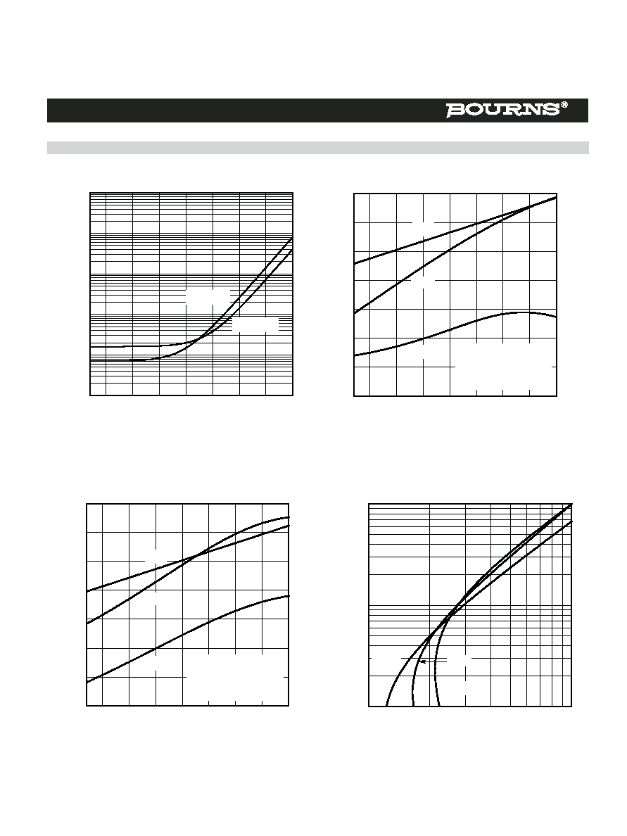
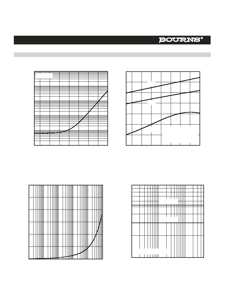
Typical Characteristics - R and G or T and G Terminals
Figure 2.
Figure 3.
Figure 4.
Figure 5.
T
J
- Junction Temperature - ∞C
-25
0
25
50
75
100
125
150
0.1
0.01
0.001
1
10
100
TC3HAF
V
D
= -50 V
V
D
= 50 V
T
J
- Junction Temperature - ∞C
-25
0
25
50
75
100
125
150
Norma
l
i
zed Br
e
akdo
w
n
V
o
l
t
ages
0.9
1.0
1.1
1.2
TC3HAI
V
(BO)
V
(BR)
V
(BR)M
T
J
- Junction Temperature - ∞C
-25
0
25
50
75
100
125
150
Normal
i
z
ed Breakdow
n V
o
l
t
ages
0.9
1.0
1.1
1.2
TC3HAJ
V
(BO)
V
(BR)
V
(BR)M
V
T
- On-State Voltage - V
2
3
4
5
6
7 8 9
1
10
I
T
-
On
-S
ta
te
Cu
rrent
-
A
1
10
100
TC3HAL
-40 ∞C
150 ∞C
25 ∞C
OFF-STATE CURRENT
vs
JUNCTION TEMPERATURE
OFF-STATE CURRENT
vs
ON-STATE VOLTAGE
NORMALIZED BREAKDOWN VOLTAGES
vs
JUNCTION TEMPERATURE
NORMALIZED BREAKDOWN VOLTAGES
vs
JUNCTION TEMPERATURE
Positive Polarity
Normalized to V
(BR)
I
(BR)
= 100 µA and 25 ∞C
Negative Polarity
Normalized to V
(BR)
I
(BR)
= 100 µA and 25 ∞C
TISP3xxxF3 (HV) Overvoltage Protector Series
MARCH 1994 - REVISED MARCH 2006
Specifications are subject to change without notice.
Customers should verify actual device performance in their specific applications.
TISP3xxxF3 (HV) Overvoltage Protector Series
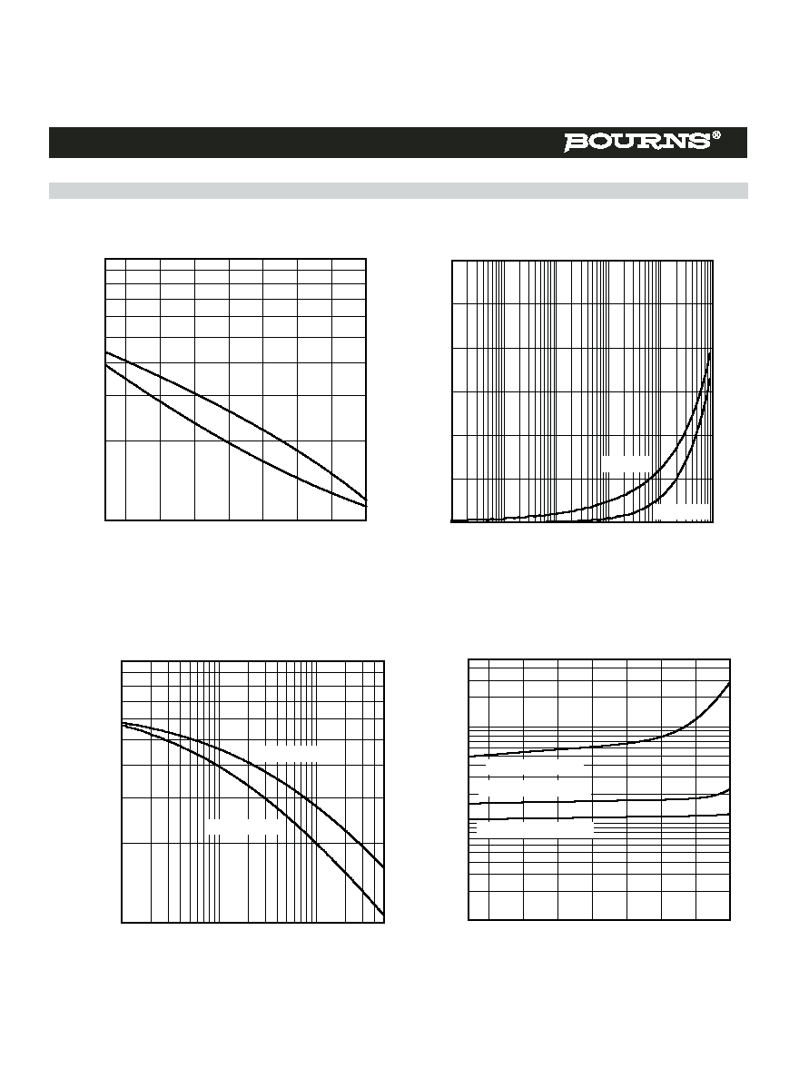
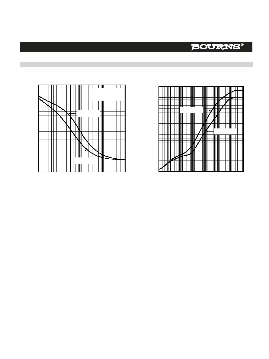
Typical Characteristics - R and G or T and G Terminals
Figure 6.
Figure 7.
Figure 8.
Figure 9.
T
J
- Junction Temperature - ∞C
-25
0
25
50
75
100
125
150
I
H
, I
(BO
)
-
Hol
di
ng Curr
ent,
Br
eakove
r
Cu
rr
ent -
A
0.2
0.3
0.4
0.5
0.6
0.7
0.8
0.9
0.1
1.0
TC3HAH
I
(BO)
I
H
di/dt - Rate of Rise of Principle Current - A/ s
0∑001
0∑01
0∑1
1
10
100
N
o
rm
al
i
z
e
d
Br
ea
kove
r
V
o
l
t
age
1.0
1.1
1.2
1.3
TC3HAB
Positive
Negative
Terminal Voltage - V
0∑1
1
10
Of
f-
S
t
at
e Capaci
tance
- pF
10
100
TC3HAE
50
Positive Bias
Negative Bias
T
J
- Junction Temperature - ∞C
-25
0
25
50
75
100
125
150
Of
f-S
t
ate
Cap
aci
tan
c
e
-
pF
1
10
100
TC3HAD
500
Terminal Bias = 0
Terminal Bias = 50 V
Terminal Bias = -50 V
HOLDING CURRENT & BREAKDOWN CURRENT
vs
JUNCTION TEMPERATURE
OFF-STATE CAPACITANCE
vs
JUNCTION TEMPERATURE
NORMALIZED BREAKOVER VOLTAGES
vs
JUNCTION TEMPERATURE
OFF-STATE CAPACITANCE
vs
TERMINAL VOLTAGE
µ

MARCH 1994 - REVISED MARCH 2006
Specifications are subject to change without notice.
Customers should verify actual device performance in their specific applications.
TISP3xxxF3 (HV) Overvoltage Protector Series
Typical Characteristics - R and G or T and G Terminals
Figure 10.
Decay Time - s
10
100
1000
M
axi
mum
S
u
rge Curr
ent
- A
10
100
1000
TC3HAA
2
SURGE CURRENT
vs
DECAY TIME
µ
MARCH 1994 - REVISED MARCH 2006
Specifications are subject to change without notice.
Customers should verify actual device performance in their specific applications.
TISP3xxxF3 (HV) Overvoltage Protector Series
Typical Characteristics - R and T Terminals
Figure 11.
Figure 12.
Figure 13.
Figure 14.
T
J
- Junction Temperature - ∞C
-25
0
25
50
75
100
125
150
I
D
- O
f
f
-
S
t
at
e
Current -
µ
A
0∑001
0∑01
0∑1
1
10
100
TC3HAG
V
D
= ±50 V
T
J
- Junction Temperature - ∞C
-25
0
25
50
75
100
125
150
Norma
l
i
zed Br
e
akdo
w
n V
o
l
t
ages
0.9
1.0
1.1
1.2
TC3HAK
V
(BO)
V
(BR)
V
(BR)M
Both Polarities
Normalized to V
(BR)
I
(BR)
= 100 µA and 25 ∞C
di/dt - Rate of Rise of Principle Current - A/µs
0∑001
0∑01
0∑1
1
10
100
N
o
rm
al
i
z
e
d
Brea
kov
er Vol
t
age
1.0
1.1
1.2
1.3
TC3HAC
Terminal Voltage - V
0∑1
1
10
O
ff-S
ta
te
C
a
pa
c
i
ta
nc
e
- fF
20
30
40
50
60
70
80
90
10
100
TC3XAA
50
D Package
SL Package
Both Voltage Polarities
OFF-STATE CURRENT
vs
JUNCTION TEMPERATURE
OFF-STATE CAPACITANCE
vs
TERMINAL VOLTAGE
NORMALIZED BREAKDOWN VOLTAGES
vs
JUNCTION TEMPERATURE
NORMALIZED BREAKOVER VOLTAGES
vs
RATE OF RISE OF PRINCIPLE CURRENT
MARCH 1994 - REVISED MARCH 2006
Specifications are subject to change without notice.
Customers should verify actual device performance in their specific applications.
TISP3xxxF3 (HV) Overvoltage Protector Series
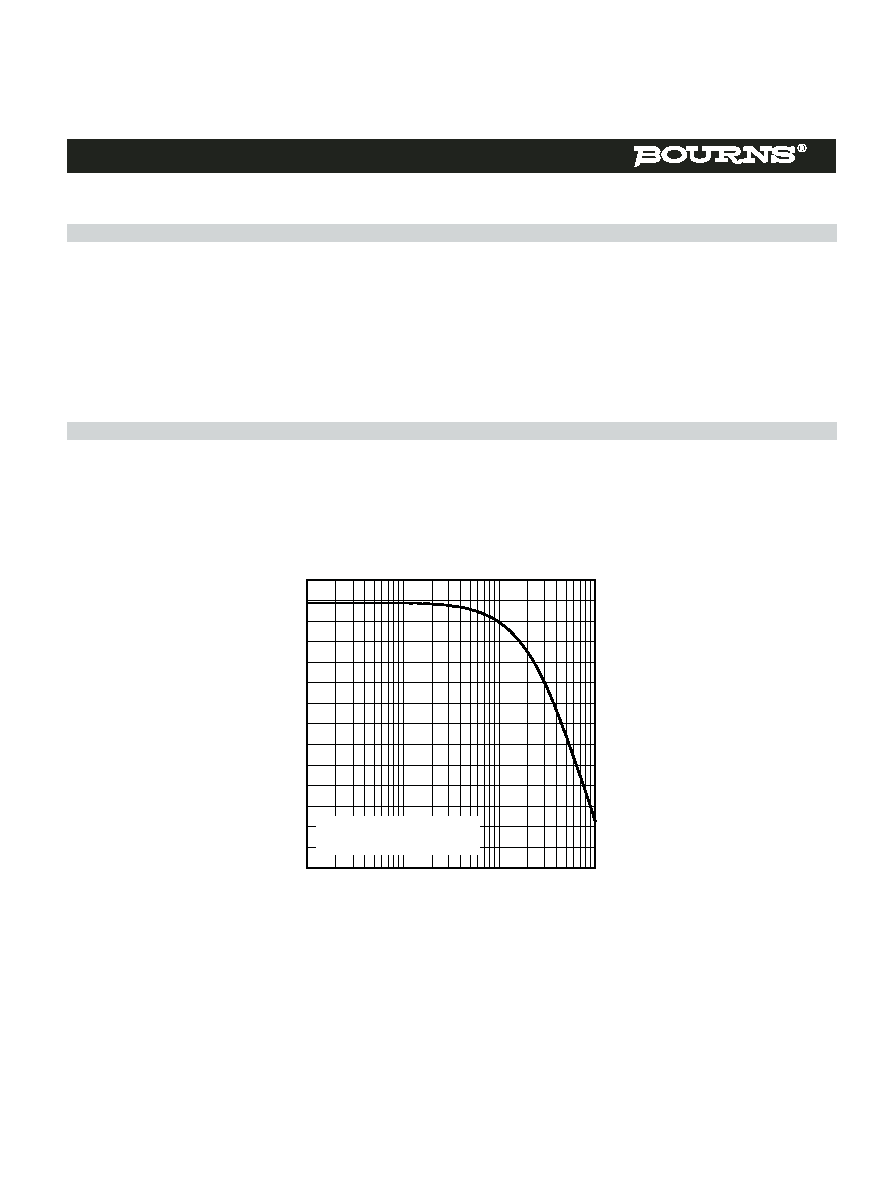
Thermal Information
Figure 15.
Figure 16.
t - Current Duration - s
0 1
.
1
10
100
1000
I
TR
M
S
-
M
a
xi
m
u
m
N
o
n
-
Recur
ren
t
50 Hz
C
u
r
r
en
t
-
A
1
10
D Package
TI3HAA
SL Package
V
GEN
= 350 Vrms
R
GEN
= 20 to 250
t - Power Pulse Duration - s
0∑0001 0∑001
0∑01
0∑1
1
10
100
1000
Z
J
A
-
T
r
ansi
ent
T
h
e
r
mal
Imp
e
d
a
n
ce -
∞C/W
1
10
100
D Package
SL Package
TI3MAA
MAXIMUM NON-RECURRING 50 Hz CURRENT
vs
CURRENT DURATION
THERMAL RESPONSE
MARCH 1994 - REVISED MARCH 2006
Specifications are subject to change without notice.
Customers should verify actual device performance in their specific applications.
TISP3xxxF3 (HV) Overvoltage Protector Series
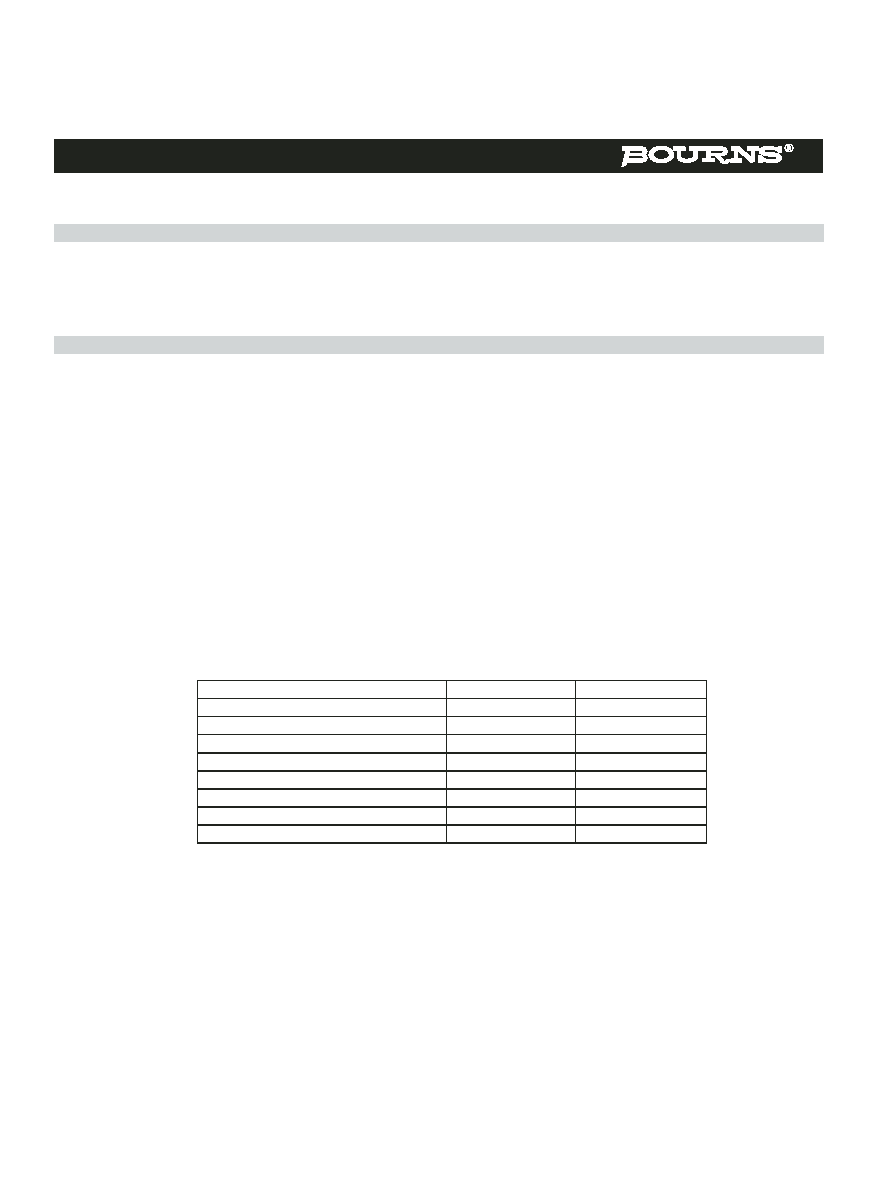
APPLICATIONS INFORMATION
Electrical Characteristics
The electrical characteristics of a TISP
Æ
device are strongly dependent on junction temperature, TJ. Hence, a characteristic value will
depend on the junction temperature at the instant of measurement. The values given in this data sheet were measured on commercial
testers, which generally minimize the temperature rise caused by testing. Application values may be calculated from the parameters'
temperature coefficient, the power dissipated and the thermal response curve, Z (see M. J. Maytum, "Transient Suppressor Dynamic
Parameters." TI Technical Journal, vol. 6, No. 4, pp. 63-70, July-August 1989).
Lightning Surge
Wave Shape Notation
Most lightning tests, used for equipment verification, specify a unidirectional sawtooth waveform which has an exponential rise and an
exponential decay. Wave shapes are classified in terms of peak amplitude (voltage or current), rise time and a decay time to 50 % of
the maximum amplitude. The notation used for the wave shape is amplitude, rise time/decay time. A 50 A, 5/310 µs wave shape would
have a peak current value of 50 A, a rise time of 5 µs and a decay time of 310 µs. The TISP
Æ
surge current graph comprehends the
wave shapes of commonly used surges.
Generators
There are three categories of surge generator type, single wave shape, combination wave shape and circuit defined. Single wave shape
generators have essentially the same wave shape for the open circuit voltage and short circuit current (e.g. 10/1000 µs open circuit
voltage and short circuit current). Combination generators have two wave shapes, one for the open circuit voltage and the other for the
short circuit current (e.g. 1.2/50 µs open circuit voltage and 8/20 µs short circuit current). Circuit specified generators usually equate to
a combination generator, although typically only the open circuit voltage waveshape is referenced (e.g. a 10/700 µs open circuit voltage
generator typically produces a 5/310 µs short circuit current). If the combination or circuit defined generators operate into a finite resis-
tance, the wave shape produced is intermediate between the open circuit and short circuit values.
Current Rating
When the TISP
Æ
device switches into the on-state it has a very low impedance. As a result, although the surge wave shape may be
defined in terms of open circuit voltage, it is the current wave shape that must be used to assess the required TISP
Æ
surge capability.
As an example, the ITU-T K.21 1.5 kV, 10/700 µs open circuit voltage surge is changed to a 38 A, 5/310 µs current waveshape when
driving into a short circuit. Thus, the TISP
Æ
surge current capability, when directly connected to the generator, will be found for the
ITU-T K.21 waveform at 310 µs on the surge graph and not 700 µs. Some common short circuit equivalents are tabulated below:
Any series resistance in the protected equipment will reduce the peak circuit current to less than the generators' short circuit value.
A 1 kV open circuit voltage, 100 A short circuit current generator has an effective output impedance of 10 (1000/100). If the
equipment has a series resistance of 25 , then the surge current requirement of the TISP
Æ
device becomes 29 A (1000/35) and not
100 A.
Standard
Open Circuit Voltage
Short Circuit Current
ITU-T K.21
1.5 kV, 10/700 µs
37.5 A, 5/310 µs
ITU-T K.20
1 kV, 10/700 µs
25 A, 5/310 µs
IEC 61000-4-5, combination wave generator
1.0 kV, 1.2/50 µs
500 A, 8/20 µs
Telcordia GR-1089-CORE
1.0 kV, 10/1000 µs
100 A, 10/1000 µs
Telcordia GR-1089-CORE
2.5 kV, 2/10 µs
500 A, 2/10 µs
FCC Part 68, Type A
1.5 kV, <10/>160 µs
200 A,<10/>160 µs
FCC Part 68, Type A
800 V, <10/>560 µs
100 A,<10/>160 µs
FCC Part 68, Type B
1.5 kV, 9/720 µs
37.5 A, 5/320 µs
MARCH 1994 - REVISED MARCH 2006
Specifications are subject to change without notice.
Customers should verify actual device performance in their specific applications.
TISP3xxxF3 (HV) Overvoltage Protector Series
APPLICATIONS INFORMATION
Protection Voltage
The protection voltage, (V
(BO)
), increases under lightning surge conditions due to thyristor regeneration. This increase is dependent on
the rate of current rise, di/dt, when the TISP
Æ
device is clamping the voltage in its breakdown region. The V
(BO)
value under surge
conditions can be estimated by multiplying the 50 Hz rate V
(BO)
(250 V/ms) value by the normalized increase at the surge's di/dt (Figure
7 ). An estimate of the di/dt can be made from the surge generator voltage rate of rise, dv/dt, and the circuit resistance.
As an example, the ITU-T K.21 1.5 kV, 10/700 µs surge has an average dv/dt of 150 V/µs, but, as the rise is exponential, the initial dv/dt
is higher, being in the region of 450 V/µs. The instantaneous generator output resistance is 25 . If the equipment has an additional
series resistance of 20 , the total series resistance becomes 45 . The maximum di/dt then can be estimated as 450/45 = 10 A/µs. In
practice, the measured di/dt and protection voltage increase will be lower due to inductive effects and the finite slope resistance of the
TISP
Æ
breakdown region.
Capacitance
Off-state Capacitance
The off-state capacitance of a TISP
Æ
device is sensitive to junction temperature, T
J
, and the bias voltage, comprising of the d.c. voltage,
V
D
, and the a.c. voltage, V
d
. All the capacitance values in this data sheet are measured with an a.c. voltage of 100 mV. The typical 25 ∞C
variation of capacitance value with a.c. bias is shown in Figure 17. When V
D
>> V
d
, the capacitance value is independent on the value of
V
d
. The capacitance is essentially constant over the range of normal telecommunication frequencies.
Figure 17.
V
d
- RMS AC Test Voltage - mV
1
10
100
1000
Normal
i
z
ed Capaci
tance
0.70
0.75
0.80
0.85
0.90
0.95
1.00
1.05
AIXXAA
Normalized to V
d
= 100 mV
DC Bias, V
D
= 0
NORMALIZED CAPACITANCE
vs
RMS AC TEST VOLTAGE
MARCH 1994 - REVISED MARCH 2006
Specifications are subject to change without notice.
Customers should verify actual device performance in their specific applications.
TISP3xxxF3 (HV) Overvoltage Protector Series
APPLICATIONS INFORMATION
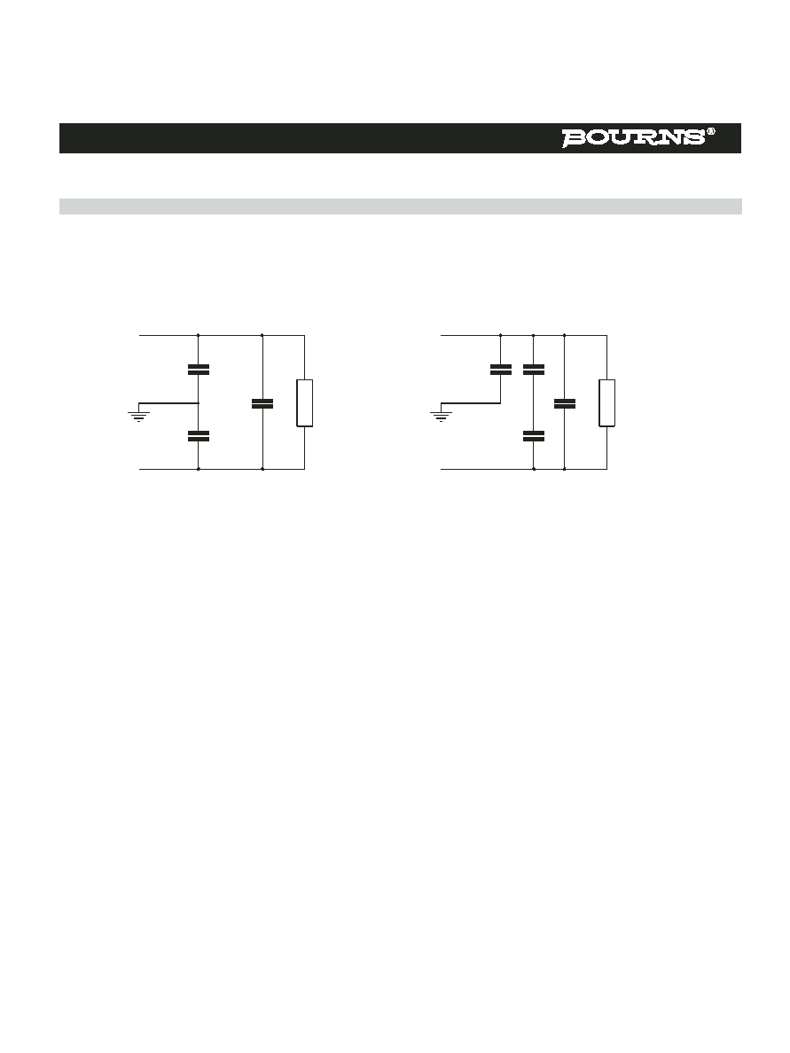
Longitudinal Balance
Figure 18 shows a three terminal TISP
Æ
device with its equivalent "delta" capacitance. Each capacitance, C
TG
, C
RG
and C
TR
, is the true
terminal pair capacitance measured with a three terminal or guarded capacitance bridge. If wire R is biased at a larger potential than
wire T, then C
TG
>C
RG
. Capacitance C
TG
is equivalent to a capacitance of CRG in parallel with the capacitive difference of (C
TG
-C
R
G).
The line capacitive unbalance is due to (C
TG
-C
RG
) and the capacitance shunting the line is C
TR
+C
RG
/2.
All capacitance measurements in this data sheet are three terminal guarded to allow the designer to accurately assess capacitive
unbalance effects. Simple two terminal capacitance meters (unguarded third terminal) give false readings as the shunt capacitance via
the third terminal is included.
Figure 18.
C
TG
C
RG
C
TR
Equipment
T
R
G
(C
TG
-C
RG
)
C
RG
C
TR
Equipment
T
R
G
C
RG
C
TG
> C
RG
Equivalent Unbalance
AIXXAB
"TISP" is a trademark of Bourns, Ltd., a Bourns Company, and is Registered in U.S. Patent and Trademark Office.
"Bourns" is a registered trademark of Bourns, Inc. in the U.S. and other countries.