NOVEMBER 2001 - REVISED FEBRUARY 2005
Specifications are subject to change without notice.
Customers should verify actual device performance in their specific applications.
TISP43xxMMAJ/BJ Overvoltage Protector Series
TISP4300MMAJ, TISP4350MMAJ, TISP4360MMAJ
TISP4300MMBJ, TISP4350MMBJ, TISP4360MMBJ
BIDIRECTIONAL THYRISTOR OVERVOLTAGE PROTECTORS
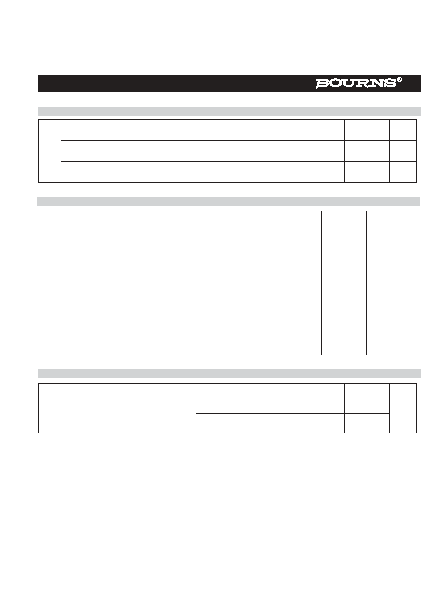
Device Symbol
Specified for:
- ITU-T Recommendation K.21
10/700
AC Induction and Contact
- FCC Part 68 (TIA/EIA-IS-968)
Type A & B Surge
- UL 60950 and CSA 22.2 No.60950
Clause 6. Power Cross
- Telcordia GR-1089-CORE
2/10 and 10/1000
AC Induction and Contact
Applications:
TISP4300MM for:
POTS Solid-State Relay Modems
Protection Voltage .............................................................. 300 V
TISP4350MM for:
POTS Electro-mechanical Relay Modems
FCC Type B Ringer Voltage ............................................... 275 V
TISP4360MM for:
ADSL Modems
ADSL + Type B Ringer Voltage .......................................... 290 V
Ion-Implanted Breakdown Region
Precise and Stable Voltage
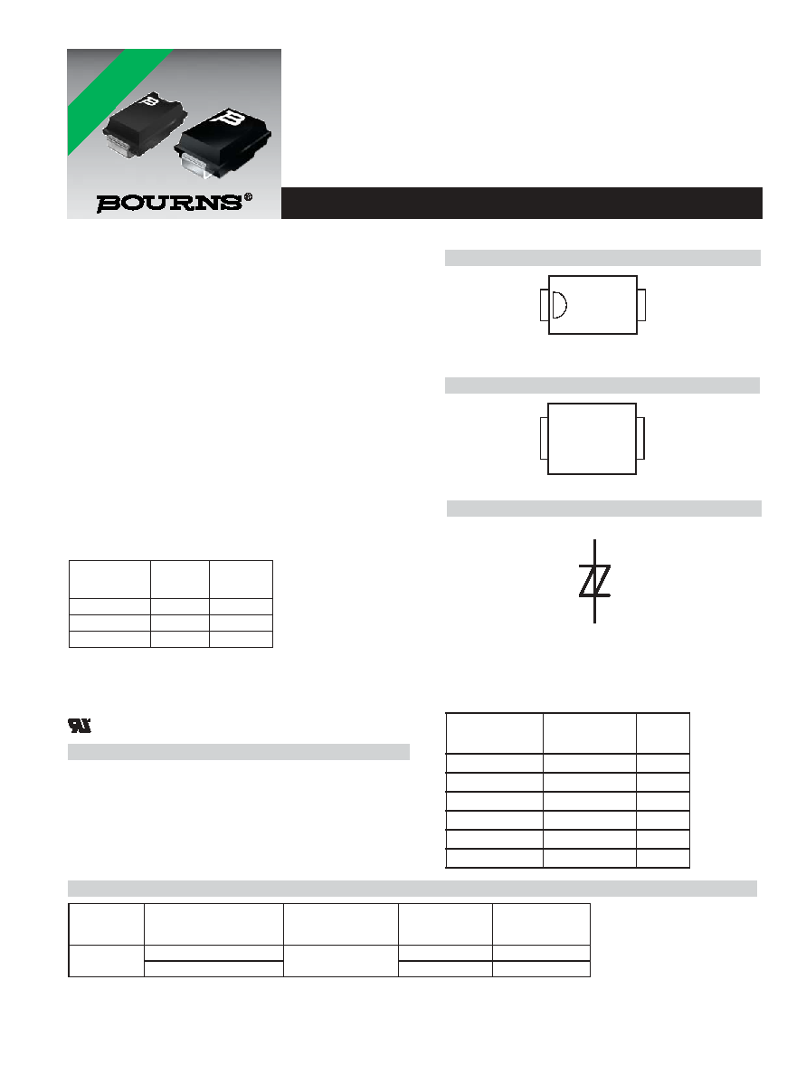
SMA Package (Top View)
Description
These devices are designed to limit overvoltages on the telephone
line. Overvoltages are normally caused by a.c. power system or
lightning flash disturbances which are induced or conducted on to the
telephone line. A single device provides 2-point protection and is
typically used for the protection of 2-wire telecommunication
equipment (e.g. between the Ring and Tip wires for telephones and
modems). Combinations of devices can be used for multi-point
protection (e.g. 3-point protection between Ring, Tip and Ground).
How To Order
Available in SMA and SMB Packages
SMA Saves 25 % Placement Area Over SMB
FCC Part 68 Type A Surge Compliance by
Using Either a Fuse or 7 Resistor
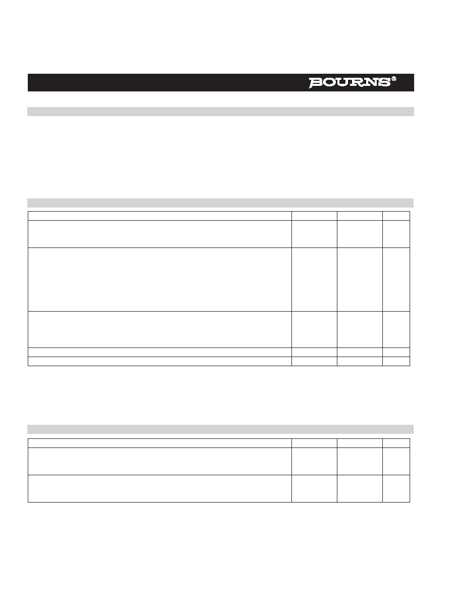
SMB Package (Top View)
Device
V
DRM
V
V
(BO)
V
`4300
230
300
`4350
275
350
`4360
290
360
MDXXCCE
1
2
R (B)
T (A)
T(A)
R(B)
MDXXBGF
2
1
T
R
SD4XAA
T
erminals T and R correspond to the
alternative line designators of A and B
Rated for International Surge Wave Shapes
Wave Shape
Standard
I
TSP
A
2/10
µ
s
GR-1089-CORE
250
10/160
µ
s
FCC Part 68
75
9/720
µ
s
FCC Part 68
65
10/700
µ
s
ITU-T K.20/45/ 21
65
10/560
µ
s
FCC Part 68
55
10/1000
µ
s
GR-1089-CORE
50
............................................ UL Recognized Components
*RoHS Directive 2002/95/EC Jan 27 2003 including Annex
Device
Package
Carrier
TISP43xxMM
SMA/DO-214AC J-Bend (AJ)
Embossed Tape Reeled
(R)
TISP43xxMMAJR
SMB/DO-214AA J-Bend (BJ)
TISP43xxMMBJR
TISP43xxMMAJR-S
TISP43xxMMBJR-S
For Standard
Termination Finish
Order As
For Lead Free
Termination Finish
Order As
*RoHS COMPLIANT
VERSIONS
AVAILABLE
NOVEMBER 2001 - REVISED FEBRUARY 2005
Specifications are subject to change without notice.
Customers should verify actual device performance in their specific applications.
TISP43xxMMAJ/BJ Overvoltage Protector Series
Description (Continued)
Overload Ratings, TA = 25 ∞C (Unless Otherwise Noted)
Absolute Maximum Ratings, TA = 25 ∞C (Unless Otherwise Noted)
The protector consists of a symmetrical voltage-triggered bidirectional thyristor. Overvoltages are initially clipped by breakdown clamping until
the voltage rises to the breakover level, which causes the device to crowbar into a low-voltage on state. This low-voltage on state causes the
current resulting from the overvoltage to be safely diverted through the device. The high crowbar holding current prevents d.c. latchup as the
diverted current subsides.
This TISP43xxMM range consists of three voltage variants targeted at specific applications: ADSL, electro-mechanical hook switch and solid
state hook switch modems. These parts are guaranteed to voltage limit and withstand the listed international lightning surges in both
polarities. Two packages are available; SMB (JEDEC DO-214AA with J-bend leads) and SMA (JEDEC DO-214AC with J-bend leads). These
devices are supplied in embossed tape reel carrier pack. For alternative voltage and holding current values, consult the factory.
Rating
Symbol
Value
Unit
Repetitive peak off-state voltage,
`4300
`4350
`4360
V
DRM
±
230
±
275
±
290
V
Non-repetitive peak on-state pulse current (see Notes 2, 3 and 4)
I
TSP
A
2/10
µ
s (GR-1089-CORE, 2/10
µ
s voltage wave shape)
250
10/160
µ
s (FCC Part 68 (TIA/EIA-IS-968), 10/160
µ
s voltage wave shape)
75
5/320
µ
s (FCC Part 68 (TIA/EIA-IS-968), 9/720
µ
s voltage wave shape)
65
5/310
µ
s (ITU-T K.44, 10/700
µ
s voltage wave shape used in K.20/45/21)
65
10/560
µ
s (FCC Part 68 (TIA/EIA-IS-968), 10/560
µ
s voltage wave shape)
55
10/1000
µ
s (GR-1089-CORE, 10/1000
µ
s voltage wave shape)
50
Non-repetitive peak on-state current (see Notes 2, 3 and 4)
I
TSM
18
7
1.6
A
20 ms (50 Hz) full sine wave
1 s (50 Hz) full sine wave
1000 s 50 Hz/60 Hz a.c.
Junction temperature
T
J
-40 to +150
∞
C
Storage temperature range
T
stg
-65 to +150
∞
C
NOTES: 1. For voltage values at lower temperatures derate at 0.13 %/
∞
C.
2. Initially, the TISP43xxMM must be in thermal equilibrium with T
J
= 25
∞
C.
3. The surge may be repeated after the TISP43xxMM returns to its initial conditions.
4. EIA/JESD51-2 environment and EIA/JESD51-3 PCB with standard footprint dimensions connected with 5 A rated printed wiring
track widths. Derate current values at -0.61 %/
∞
C for ambient temperatures above 25
∞
C.
Rating
Symbol
Value
Unit
Peak overload on-state current, Type A impulse (see Note 5)
I
T(OV)M
200
100
A
10/160
µ
s
10/560
µ
s
Peak overload on-state current, a.c. power cross tests UL 60950 (see Note 5)
I
T(OV)M
See Figure 10
for current
versus time
A
NOTE
5: These electrical stress levels may damage the TISP43xxMM silicon chip. After test, the pass criterion is either that the device is
functional or, if it is faulty, that it has a short circuit fault mode. In the short circuit fault mode, the following equipment is protected
as the device is a permanent short across the line. The equipment would be unprotected if an open circuit fault mode developed.
NOVEMBER 2001 - REVISED FEBRUARY 2005
Specifications are subject to change without notice.
Customers should verify actual device performance in their specific applications.
TISP43xxMMAJ/BJ Overvoltage Protector Series
Recommended Operating Conditions
Electrical Characteristics for the R and T Terminals, TA = 25 ∞C (Unless Otherwise Noted)
Component
Min
Typ
Max
Unit
R
S
series resistor for FCC Part 68, 10/160, 10/560 type A surge survival
13
series resistor for FCC Part 68, 9/720 type B surge survival
0
series resistor for GR-1089-CORE first-level and second-level surge survival
15
series resistor for K.20, K.21 and K.45 1.5 kV, 10/700 surge survival
0
series resistor for K.21 coordination with a 400 V primary protector
6.6
Parameter
Test Conditions
Min
Typ
Ma x
Unit
I
DRM
Repetitive peak off-
state current
V
D
= V
DRM
T
A
= 25
∞
C
T
A
= 85
∞
C
±
5
±
10
µ
A
V
(BO)
Breakover voltage
dv/dt =
±
250 V/ms,
R
SOURCE
= 300
`4300
`4350
`4360
±
300
±
350
±
360
V
I
(BO)
Breakover current
dv/dt =
±
250 V/ms,
R
SOURCE
= 300
±
0.8
A
I
H
Holding current
I
T
=
±
5 A, di/dt = -/+30 mA/ms
±
0.15
±
0.6
A
dv/dt
Critical rate of rise of
off-state voltage
Linear voltage ramp, Maximum ramp value < 0.85V
DRM
±
5
kV/
µ
s
I
D
Off-state current
`4300, V
D
=
±
207 V
`4350, V
D
=
±
248 V
`4360, V
D
=
±
261 V
±
2
µ
A
I
D
Off-state current
V
D
=
±
50 V
±
10
±
10
C
off
Off-state capacitance
f = 1 MHz, V = 1 V rms, V
D
D
d
d
=
±
1 V
f = 1 MHz, V = 1 V rms, V =
±
50 V
40
18
pF
Thermal Characteristics
Test Conditions
Parameter
Min
Typ
Max
Unit
R
JA
Junctio n to free air thermal resistance
EIA/JESD51-3 PCB, I
T
= I
TSM(1000)
,
T
A
= 25
∞
C, (see Note 6)
115
∞
C/W
265 mm x 210 mm populated line card,
4-layer PCB, I
T
= I
TSM(1000)
, T
A
= 25
∞
C
52
NOTE
6: EIA/JESD51-2 environment and PCB has standard footprint dimensions connected with 5 A rated printed wiring track widths.
NOVEMBER 2001 - REVISED FEBRUARY 2005
Specifications are subject to change without notice.
Customers should verify actual device performance in their specific applications.
TISP43xxMMAJ/BJ Overvoltage Protector Series
Parameter Measurement Information
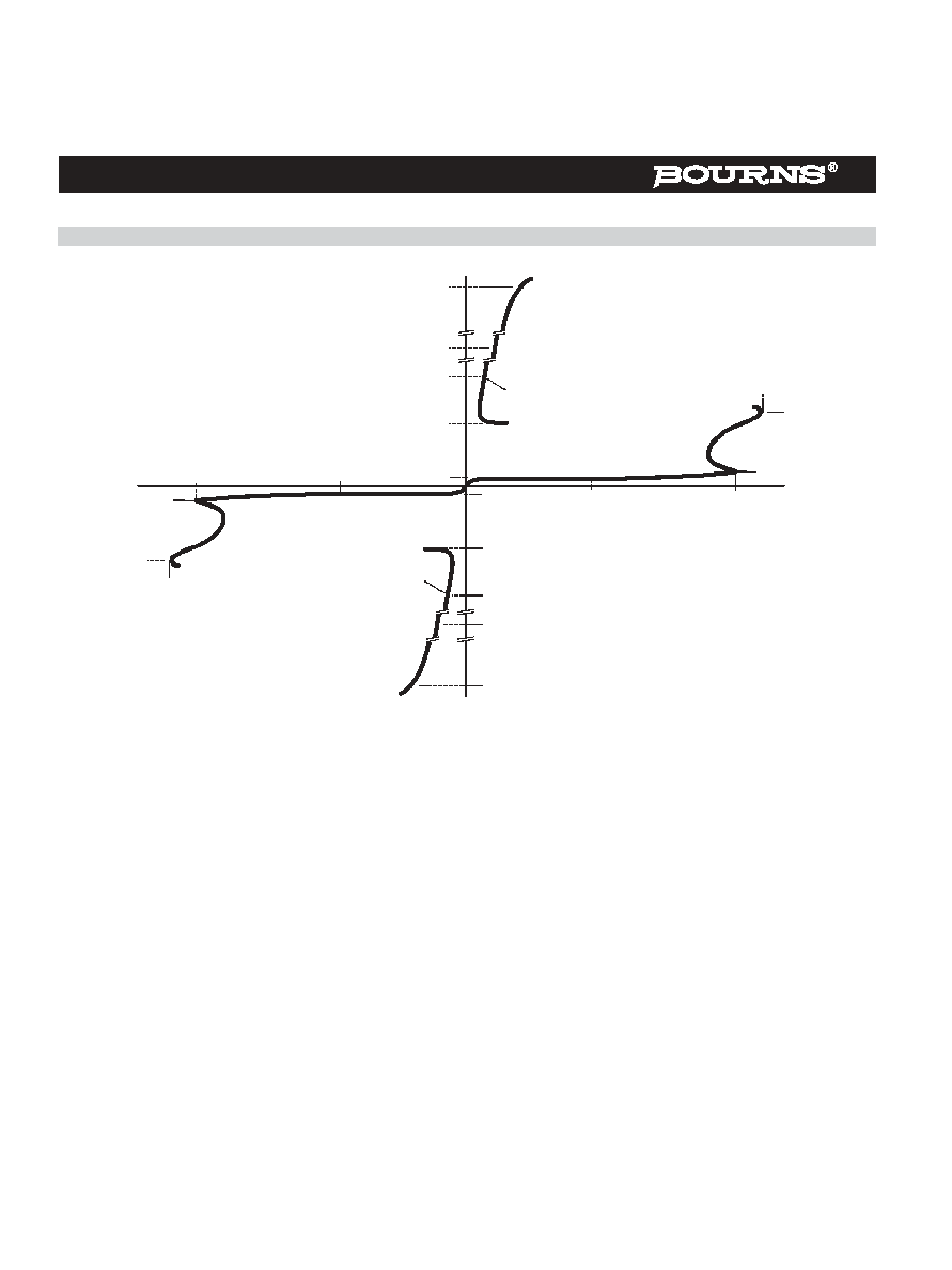
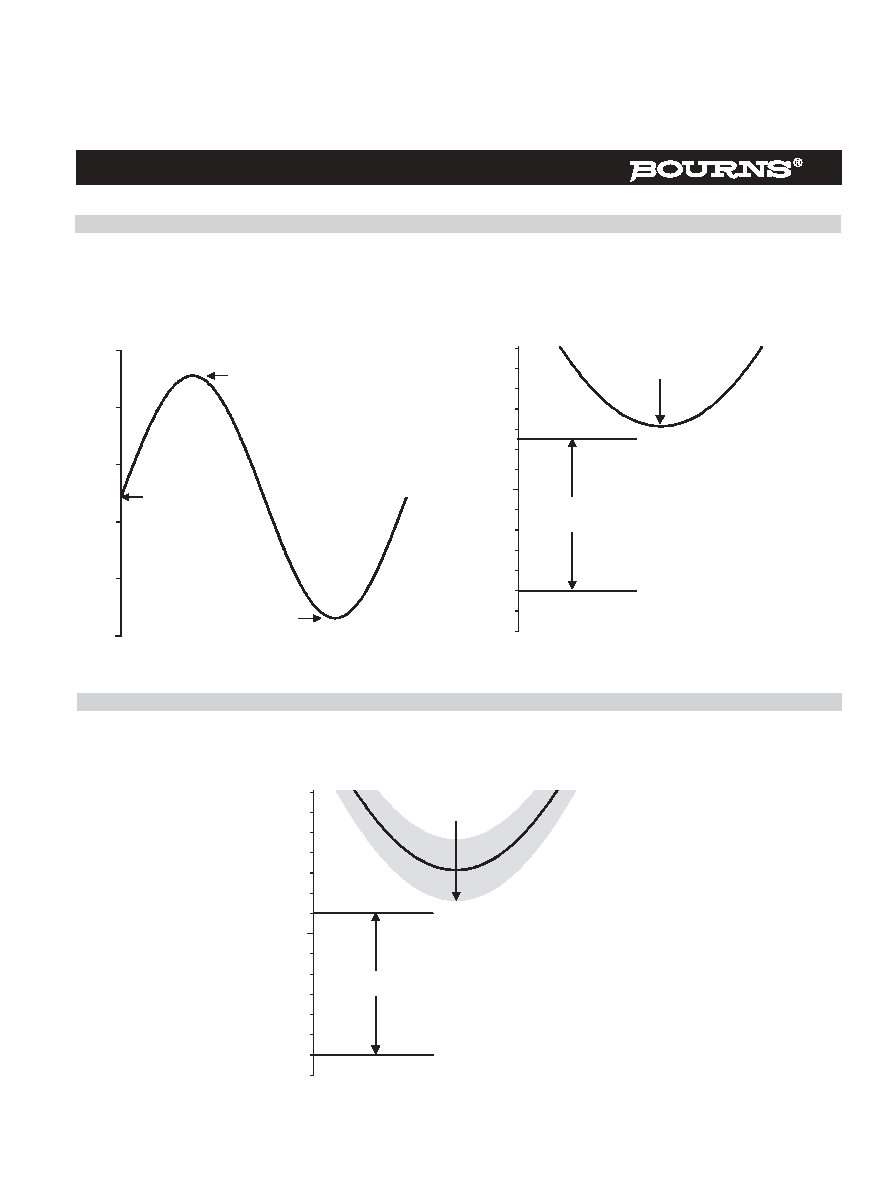
Figure 1. Voltage-current Characteristic for T and R Terminals
All Measurements are Referenced to the R Terminal
-v
V
DRM
I
DRM
V
D
I
H
I
T
V
T
I
TSM
I
TSP
V
(BO)
I
(BO)
I
D
Quadrant I
Switching
Characteristic
+v
+i
V
(BO)
I
(BO)
V
D
I
D
I
H
I
T
V
T
I
TSM
I
TSP
-i
Quadrant III
Switching
Characteristic
PMXXAAB
V
DRM
I
DRM
NOVEMBER 2001 - REVISED FEBRUARY 2005
Specifications are subject to change without notice.
Customers should verify actual device performance in their specific applications.
TISP43xxMMAJ/BJ Overvoltage Protector Series
Typical Characteristics
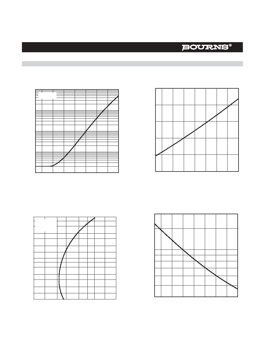
Figure 2.
OFF-STATE CURRENT
vs
JUNCTION TEMPERATURE
T
J
- Junction Temperature -
∞
C
-25
0
25
50
75
100
125
150
|I
D
|
-
Off-State Current -
µ
A
0∑001
0∑01
0∑1
1
10
TC4LAG
V
D
=
±
50 V
Figure 3.
NORMALIZED BREAKOVER VOLTAGE
vs
JUNCTION TEMPERATURE
T
J
- Junction Temperature -
∞
C
-25
0
25
50
75
100
125
150
Normaliz
ed Break
o
ver
V
olta
g
e
0.90
0.95
1.00
1.05
1.10
1.15
TC4LAF
Figure 4.
ON-STATE CURRENT
vs
ON-STATE VOLT AGE
V
T
- On-State Voltage - V
0.7
1.5
2
3
4
5
7
1
1
0
I
T
-
On-State Current - A
0.5
0.7
1.5
2
3
4
5
7
15
20
30
40
50
1
10
T
A
= 25
∞
C
t
W
= 100
µ
s
TC4MAN
Figure 5.
NORMALIZED HOLDING CURRENT
vs
JUNCTION TEMPERATURE
T
J
- Junction Temperature -
∞
C
-25
0
25
50
75
100
125
150
Normaliz
ed Holding Current
0.4
0.5
0.6
0.7
0.8
0.9
1.5
2.0
1.0
TC4LAD
NOVEMBER 2001 - REVISED FEBRUARY 2005
Specifications are subject to change without notice.
Customers should verify actual device performance in their specific applications.
TISP43xxMMAJ/BJ Overvoltage Protector Series
Typical Characteristics
Figure 6.
NORMALIZED CAPACITANCE
vs
OFF-STATE VOLTAGE
V
D
- Off-state Voltage - V
0.5
1
2
3
5
10
20 30
50
100150
Capacitance Normaliz
ed to
V
D
= 0
0.2
0.3
0.4
0.5
0.6
0.7
0.8
0.9
1
TC4LAH
T
J
= 25
∞
C
V
d
= 1 Vrms
Figure 7.
TYPICAL CAPACI TANCE ASYMMETRY
vs
OFF-STATE VOLTAGE
V
D
-- Off-State Voltage ≠ V
2
3
4 5
7
20
30 40 50
1
1
0
|C
off
(
+VD
)
- C
off
(
-VD
)
|
--
Capacitance Asymmetr
y ≠ pF
0
1
V
d
= 1 V rms, 1 MHz
V
d
= 10 mV rms, 1 MHz
TC4LBB
NOVEMBER 2001 - REVISED FEBRUARY 2005
Specifications are subject to change without notice.
Customers should verify actual device performance in their specific applications.
TISP43xxMMAJ/BJ Overvoltage Protector Series
Rating and Thermal Information
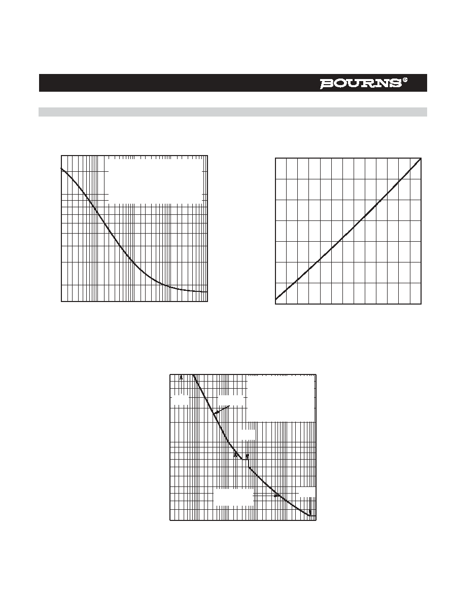
Figure 8.
NON-REPETITIVE PEAK ON-STATE CURRENT
vs
CURRENT DURATION
t - Current Duration - s
0.01
0.1
1
10
100
I
TSM(t)
-
Non-Repetitive P
eak On-State Current - A
1.5
2
3
4
5
6
7
8
9
15
20
10
TI4LAI
V
GEN
= 600 Vrms, 50/60 Hz
R
GEN
= 1.4*V
GEN
/I
TSM(t)
EIA/JESD51-2 ENVIRONMENT
EIA/JESD51-3 PCB
T
A
= 25
∞
C
Figure 9.
V
DRM
DERATING FACTOR
vs
MINIMUM AMBIENT TEMPERATURE
T
AMIN
- Minimum Ambient Temperature -
∞
C
-35
-25
-15
-5
5
15
25
-40
-30
-20
-10
0
10
20
Derating F
actor
0.93
0.94
0.95
0.96
0.97
0.98
0.99
1.00
TI4LAE
Figure 10. Peak Overload On-State Current against Duration
PEAK OVERLOAD ON-STATE CURRENT
vs
CURRENT DURATION
t - Current Duration - s
0∑01
0∑1
1
10
100
1000
I
T(
O
V
)
M
--
P
eak Overload On-State Current -- A rms
2
2.5
3
3.5
4
5
6
7
8
9
15
20
25
30
35
40
10
TI4MAM
40 A
100 A
2
s
2.2 A
7 A
WIRING
SIMULATOR
DEVICE WILL
CARRY CURRENT
OF TESTS 1 THRU 5
CLAUSE 6.4, UL 60950,
FOR FULL TEST TIME
NOVEMBER 2001 - REVISED FEBRUARY 2005
Specifications are subject to change without notice.
Customers should verify actual device performance in their specific applications.
APPLICATIONS INFORMATION
TISP43xxMMAJ/BJ Overvoltage Protector Series
FCC Part 68, ACTA, TIA and EIA
Fuse Values for TIA/EIA-IS-968 (FCC Part 68)
Fuses must not operate on the Type B surge. To survive a 37.5 A Type B surge, the fuse needs to have a melting I
2
t of greater than 0.7 A
2
s.
To survive the Type A surges a fuse melting I
2
t value of greater than 10 A
2
s for 10/160 and 8 A
2
s for 10/560 is needed. By using a fuse which
does not operate on Type B surges (I
2
t > 0.7 A
2
s) and does operate on Type A surges (I
2
t < 8 A
2
s) a non-operational pass can be achieved for
Type A testing.
From 2001, the registrations for FCC equipment changed from the FCC to ACTA, Administrative Council for Terminal Attachments. For this
function, ACTA needed to adopt a US National standard specifying terminal equipment requirements. The TIA, Telecommunications
Industry Association, in conjunction with the EIA, Electronic Industries Alliance, created TIA/EIA-IS-968 for this purpose. The first issue of
TIA/EIA-IS-968 is essentially a renumbered version of the FCC Part 68 requirement. Clause and figure changes are shown in the table.
Item
FCC Part 68
TIA/EIA-IS-968
Telephone Line Surge ≠ Type A
Clause 68.302 (b)
Clause 4.2.2
Telephone Line Surge ≠ Type B
Clause 68.302 (c)
Clause 4.2.3
Simplified Surge Generator
Fig. 68.302 (a)
Figure 4.1
Open Circuit voltage Wave shape
Fig. 68.302 (b)
Figure 4.2
Short Circuit Current Wave shape
Fig. 68.302 (c)
Figure 4.3
TIA/EIA-IS-968 (FCC Part 68) Impulse Testing
To verify the withstand capability and safety of the equipment, standards require that the equipment is tested with various impulse wave forms.
The table below shows values for the TIA/EIA-IS-968 and ITU-T recommendation K.21.
Standard
Test
Condition
V
Peak
Voltage
V
Voltage
Wave Form
µs
Peak
Current
A
Current
Wave Form
µs
Fictive
Impedance
TISP43xxMM
Rating
A
Series
Resistance
TIA/EIA-IS-968
(F CC Part 68)
Longitudinal
1500
10/160
200
10/160
7.5
75
2 x 13
Metallic
800
10/560
100
10/560
8
55
7
Longitudinal
1500
9/720
37.5
5/320
40
65
0
Metallic
1000
9/720
25
5/320
40
65
0
ITU-T K.21
Basic Level
Transverse
1500
4000
10/700
37.5
100
5/310
40
65
0
6.6
ITU-T K.21
Enhanced Level
Transverse
1500
6000
10/700
37.5
125
5/310
40
65
0
6.2
TIA/EIA-IS-968 terminology for the wave forms produced by the ITU-T recommendation K.21 10/700 impulse generator
Values assume the TISP43xxMM is connected inter-conductor and a 400 V primary is used
If the impulse generator current exceeds the protector's current rating then a series resistance can be used to reduce the current to the
protector's rated value to prevent possible failure. For the new edition of ITU-T recommendation K.21 (2000) some series resistance might
be needed to pass the impulse coordination test. The value for a 400 V primary protector is given in the table.
The required value of device survival series resistance for a given waveform is given by the following calculations. First, the minimum total
circuit impedance is found by dividing the impulse generator's peak voltage by the protector's rated current. The impulse generator's fictive
impedance (generator's peak voltage divided by peak short circuit current) is then subtracted from the minimum total circuit impedance to
give the required value of series resistance.
For the TIA/EIA-IS-968 10/560 waveform the following values result. The minimum total circuit impedance is 800/55 = 15 and the
generator's fictive impedance is 800/100 = 8 . For an inter-conductor connected TISP43xxMM, this gives a minimum series resistance value
of 15 - 8 = 7 . The 10/160 waveform only needs to be considered if the TISP43xxMM is connected from the conductor to ground. In this
case the conductor series resistance is 12.5 per conductor.
NOVEMBER 2001 - REVISED FEBRUARY 2005
Specifications are subject to change without notice.
Customers should verify actual device performance in their specific applications.
TISP43xxMMAJ/BJ Overvoltage Protector Series
TIA/EIA-IS-968 (FCC Part 68) System Voltage Levels
The protector should not clip or limit the voltages that occur in normal system operation. If the maximum system voltages are not known, then
designers often used the voltages for the FCC Part 68 "B" ringer. The "B" ringer has a d.c. voltage of 56.5 V and a maximum a.c. ring voltage
of 150 V rms. The resultant waveform is shown in Figure 11. The maximum voltage is -269 V, but, because of possible wiring reversals, the
protector should have a working voltage of ±269 V minimum. The TISP4350MM protector meets this requirement with a working voltage,
V
DRM
, of ±275 V and a protection voltage, V
(BO)
, of ±350 V. Figure 12 shows the TISP4350MM voltages relative to the POTS -269 V peak
ringing voltage.
ADSL System Voltage Levels
The ADSL signal can be as high as ±15 V and this adds to the POTS signal making a peak value of -284 V. This increased signal value of
-284 V would be clipped by the TISP4350MM, which only allows for a -275 V signal. The TISP4360MM has been specified to overcome this
problem by having a higher working voltage of ±290 V. Figure 13 shows the TISP4360MM voltages relative to the -284 V peak ADSL plus
POTS ringing voltage. The ±15 V ADSL signal is shown as a gray band in Figure 13.
Figure 11.
-300 V
-56.5 V d.c.
-200 V
-100 V
0
100 V
200 V
-269 V
+156 V
AI4XAD
Figure 12.
-370
-360
-350
-340
-330
-320
-310
-290
-280
-270
-260
-250
-240
-230
-300
TISP4 350MM
WORKING VOLTAGE V
DRM
PROTECTION VOLT AGE V
(BO)
AI4HAEA
-269 V
RINGING PEAK
-275 V
-350 V
Figure 13.
-370
-360
-350
-340
-330
-320
-310
-290
-280
-270
-260
-250
-240
-230
-300
PROTECTION VOLT AGE V
(BO)
-284 V PEAK
ADSL + RINGING
TISP4 360MM
WORKING VOLTAGE V
DRM
AI4HAFA
-290 V
-360 V

NOVEMBER 2001 - REVISED FEBRUARY 2005
Specifications are subject to change without notice.
Customers should verify actual device performance in their specific applications.
TISP43xxMMAJ/BJ Overvoltage Protector Series
IEC 60950, UL 1950/60950, CSA C22.2 No. 950/60950 and EN 60950
UL 60950, Clause 6.4 ≠ Power Cross
Figure 14 shows the criterion flow for UL 60950 power cross. (This is a modified version of UL60950, Figure 6C -- Overvoltage flowchart.)
There are many routes for achieving a pass result. For discussion, each criterion has been given a letter reference. Brief details of any
electrical testing is given as a criterion note. Test pass criteria are given in the bottom table of Figure 14.
These electrical safety standards for IT (Information Technology) equipment at the customer premise use the IEC (International Electro-
technical Commission) 60950 standard as the core document. The IEC 60950 covers fundamental safety criteria such as creepage and
isolation. The connection to a telecommunication network voltage (TNV) is covered in clause 6.
Europe is harmonized by CENELEC (ComitÈ EuropÈen de Normalization Electro-technique) under EN 60950 (included in the Low Voltage
Directive, CE mark). Up to the end of 2000, the US had UL (Underwriters Laboratories) 1950 and Canada CSA (Canadian Standards Authority)
C22.2 No. 950. The US and Canadian standards include regional changes and additions to the IEC 60950. A major addition is the inclusion of
clause 6.6, power cross withstand containing the flowchart Figure 18b and annex NAC covering testing. Remarks made for UL 1950 will
generally be true for CSA 22.2 No. 950.
In December 2000, UL released UL 60950, which will run concurrently with UL 1950 until 2003, after which submittals can only be made for
UL 60950. The equivalent Canadian document is designated CSA C22.2 No. 60950. Changes and differences between UL 1950 and UL
60950 do not affect power cross testing nor evaluation criteria. Clause and figure numbering has changed between the standards and these
changes are shown in the table. In this document, these two standards are being jointly referred to as UL 60950 and the clause and figure
numbering referenced will be from UL 60950.
Item
UL 1950
UL 60950
Protection against overvoltage from power line crosses
Clause 6.6
Clause 6.4
Overvoltage flowchart
Figure 18b
Figure 6C
NOVEMBER 2001 - REVISED FEBRUARY 2005
Specifications are subject to change without notice.
Customers should verify actual device performance in their specific applications.
TISP43xxMMAJ/BJ Overvoltage Protector Series
Figure 14. UL 60950 Power Cross Flow Chart
Yes
Yes
IT
Equipment
parameters
Has
100 A
2
s
@ 600 V
)
Has
1.3 A
d.c.
limiting
)
Has
fire
enclosure
Has
min.
26 AWG
supplied
cord
Pass 6.3.3
ground/line
separation
ß )
Has fire
enclosure
and
spacings
Pass Test 1
Pass test 5
Pass test 2
pass tests
3, 4
Fail
Pass
No overvoltage
testing
No
Yes
No
Yes
No
No
No
Yes
Yes
No
Yes
No
Yes
Yes
No
No
Yes
UL 60950 (12/2000)
Telecommunication network connection
Clause 6.4 -- Protection against overvoltage from power line crosses
Figure 6C -- Overvoltage flowchart
Annex NAC (normative) -- Power line crosses
Test 1.
600 V, 40 A,
1.5 s
Test 5.
120 V, 25 A,
30 min or
open circuit
Test 2.
∂ )
600 V, 7 A, 5 s
Test 3. #
)
600 V, 2.2 A,
30 min or open circuit (3A)
Test 3A.
# )
600 V, <3.3 A, 30 min, no
open circuit
Test 4. # )
< Limiting voltage, <2.2 A,
30 min, no open circuit, no
overvoltage protector
voltage limiting
NOTES
) Overcurrent protector I t must be lower than any other equipment element which carries the same current.
2
) UL accepts that a fuse with a 1 A or less rating meets the 1.3 A criterion.
ß ) Pass for 120 V a.c. between telecommunication line and ground current < 10 mA.
∂ ) Test 2 not required if the equipment d.c. breaking is 1.3 A or less, see comment ).
# ) Tests 3 and 4 not required for equipment with less than 1000 m of outside cable.
No
AIUL60950A
Pass criteria
No cheesecloth charring
Insulation OK
Wiring simulator (fuse) OK
I
2
t < 100 A
2
s @ 600 V a.c.
Test 1
Test 2
A
B
C
D
E
F
H
G
I
J
Users must verify
requirements
against latest issue
of UL 60950
Connects
to outside
cable
Test 3
Test 3A
Test 4
Test 5
NOVEMBER 2001 - REVISED FEBRUARY 2005
Specifications are subject to change without notice.
Customers should verify actual device performance in their specific applications.
TISP43xxMMAJ/BJ Overvoltage Protector Series
Power Cross Pass Routes
This discussion covers typical modem flows.
Flow
Comment
Box A
The criterion for box A is if the modem connects to an outside TNV line.
The majority of modems will be connected to an outside line, so the answer is
yes. The
yes path goes to box B.
Box B
The criterion for box B is if the equipment has a limit of
100 A
2
s at 600 V rms
for Test 1. Many interpret this as a fuse with I
2
t
100 A
2
s and often miss the
600 V a.c. breaking requirement. However, the current loop is comp leted by
the fuse and ot her equipment compon ents. To ensure that the fuse I
2
t sets
the equipment performance, the other current loop componen ts, such as the
printed wiring (PW), must have higher I
2
t values than the fuse. Certainly the
fuse I
2
t needs to be lower than 100 A
2
s but ot her compon ents, for example IC
packaging, may impose a hazard-free limit of 10 A
2
s. (This conflicts with TIA/
EIA-IS-968 Type A surge pass requirement of 8 A
2
s.)
A
yes leads to box C and a no to box E.
Boxes E and I
The criterion for box E is for a minimum telecommunications line cord of No.
26 AWG to be supplied or specified.
A
yes leads to box F and a no to box I.
The criterion for box I is to pass Test 1.
If all the four pass criteria of Test 1 are met, this is a
yes and the flow goes to
box F.
A
no result fails the equipment.
No tests
B
A
N
Y
E
B
A
C
N
Y
Y
Fail
E
F
I
N
N
Y
Y
NOVEMBER 2001 - REVISED FEBRUARY 2005
Specifications are subject to change without notice.
Customers should verify actual device performance in their specific applications.
TISP43xxMMAJ/BJ Overvoltage Protector Series
Power Cross Pass Routes (Continued)
Boxes C and D
The criterion for box C is overcurrent protection that reduces currents above
1.3 A. This requirement is met by a 1 A fuse (a 1 A current fusing rating, not an
IEC 1 A current carrying rating).
Modems which pass FCC Part 68 Type B surges and non-operationally pass
Type A surges can use a fuse of 1 A or less, so the
yes path to box D can be
followed . High performance modems which operationally pass both Type A
and B surges would need a fuse of greater than 1 A and so fol low the
no path
to box F.
The criterion for box D is a fire enclosure.
Few modems can afford fire enclosures. However, for an internal modem in a
known comp uter case, the case may be evaluated as a fire enclosure. A
successful case evaluation will give a
yes and an equipment pass.
More likely, the modem w ill not have a fire enclosure. The
no flow goes to box
H.
Boxes F and J
The criterion for box F is a pass to cl ause 6.3.3 requirements.
A
yes goes to box G and a no goes to box J.
The criterion for box J is to pass Test 5.
If all the three pass criteria of Test 5 are met, this is a
yes and the flow goes to
box G.
A
no result fails the equipment.
Boxes G and H
The criterion for box G is a fire enclosure and spacings (See box D
comments).
A
yes result passes the equipment and a no result leads to box H.
The criterion for box H is to pass Tests 2, 3 and 4. Test 2 is not required if
there is overcurrent protection that reduces currents above 1.3 A (See box C).
High performance mod ems, using fuses and without fire enclosures, must
pass tests 2, 3, possibly 3A if the fuse opens, and 4. For standard modems,
using fuses of 1 A or less and without fire enclosures, tests 3, 3A and 4 must
be passed.
If the two pass criteria of each of the tests performed are met, this is a
yes
and the equipment passes.
A
no result fails the equipment.
Flow
Comment
Pass
F
B
A
C
H
D
N
Y
Y
N
Y
Y
Fail
F
G
J
Y
N
Y
N
Y
Y
G
H
Fail
Pass
N
N

NOVEMBER 2001 - REVISED FEBRUARY 2005
Specifications are subject to change without notice.
Customers should verify actual device performance in their specific applications.
TISP43xxMMAJ/BJ Overvoltage Protector Series
Fuse Values for UL 1950/60950
Fuses for the UL 1950/60950 power cross need to break the specified currents at 600 V a.c. - ordinary fuses will not do! Fuse specification
terms like short circuit capabilities to UL 1459 and UL 1950/60950, 40 A, 7 A and 2.2 A at 600 V a.c. ensure that the 600 V breaking is met.
The requirement of Figure 14, box B, limits the fuse I
2
t to less than 100 A
2
s.
Box C, with its 1.3 A limit gives a flow division. Modems passing the TIA/EIA-IS-968 Type A surge in a non-operational mode, could use a fuse
of 1 A rating or less and satisfy the 1.3 A limit and move to box D. Modems operationally passing the Type A surge will tend to use a 1.25 A
fuse, such as the Bel SMP 1.25, and move to box F. Fuses with ratings of 2 A and above may not operate before the wiring simulator fails
(typically 3 A d.c.).
TISP43xxMM and UL 1950/60950 Power Cross
The TISP43xxMM conducts current for periods greater than the power cross test times, Figure 10, so the TISP43xxMM is not a major factor in
UL 1950/60950 compliance. The main design task for UL 1950/60950 power cross is about enclosure design and the selection of the other
components that are subject to power cross. A UL specified fuse together with a TISP43xxMM gives a simple design approach to meeting the
power cross requirements.
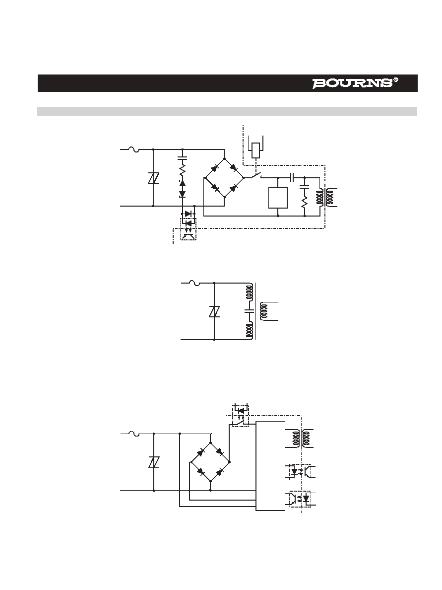
Summary of TISP4350MM, TISP4360MM and TISP4300MM Applications
The TISP4350MM is designed to meet the FCC Part 68 Type B ringer voltages and is suitable for electro-mechanical hook switch POTS
modems, Figure 15. For ADSL modems, the TISP4360MM should be used as it has an increased working voltage to avoid clipping the ADSL
signal, Figure 16. The solid state hook switch used in POTS modems may be limited in voltage and dissipation capability. To reduce the
voltage stress level on the solid state switch, a 300 V V
(BO)
TISP4300MM can be used, Figure 17.
NOVEMBER 2001 - REVISED FEBRUARY 2005
Specifications are subject to change without notice.
Customers should verify actual device performance in their specific applications.
TISP43xxMMAJ/BJ Overvoltage Protector Series
Application Circuits
Figure 15. Basic TISP4350MM Electro-Mechanical Hook Switch Protection
AI4MMAB
R
T
Ring
Detector
Hook
Switch
Polarity
Bridge
Relay
DC
Sink
Signal
C1
TISP
4350MM
Th1
Fuse or
7
Resistor
F1
R1
D5
D6
D7
OC1
Protection
D1 D2
D3 D4
Isolation Barrier
T1
C2
R2
C3
Figure 16. Basic TISP4360MM ADSL Interface
C
R
AI4MMAA
Signal
T
Tx
TISP
4360MM
Th1
Fuse or
7
Resistor
F1
Figure 17. Basic TISP4300MM Electronic Hook Switch Protection
AI4MMAC
R
T
Ring
Detector
Polarity
Bridge
Power
TISP
4300MM
Th1
Fuse or
7
Resistor
F1
Protection
Isolation Barrier
Tx Signal
Hook
Switch
Solid
State
Relay
OC1
OC2
Rx Signal
D1 D2
D3 D4
NOVEMBER 2001 - REVISED FEBRUARY 2005
Specifications are subject to change without notice.
Customers should verify actual device performance in their specific applications.
MECHANICAL DATA
TISP43xxMMAJ/BJ Overvoltage Protector Series
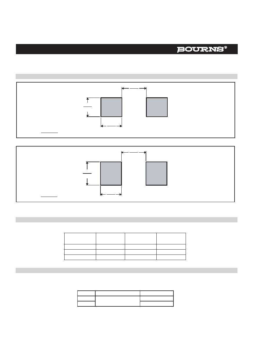
Recommended Printed Wiring Land Pattern Dimensions
Device Symbolization Code
Devices will be coded as below. As the device parameters are symmetrical, terminal 1 is not identified.
Carrier Information
Devices are shipped in one of the carriers below. Unless a specific method of shipment is specified by the customer, devices will be shipped in
the most practical carrier. For production quantities, the carrier will be embossed tape reel pack. Evaluation quantities may be shipped in bulk
pack or embossed tape.
SMA Land Pattern
MDXX BIC
2.34
(. 092)
1.90
(.075)
2.16
(.085)
DIMENSIONS ARE:
MILLIMETERS
(INCHES)
SMB Land Pattern
MDXX BIB
2.54
(.100)
2.40
(.095)
2.16
(.085)
DIMENSIONS ARE:
MILLIMETERS
(INCHES)
SMA
Package
Symbolization
Code
SMB
Package
Symbolization
Code
TISP4300MMAJ
430MM
TISP4300MMBJ
4300MM
TISP4350MMAJ
435MM
TISP4350MMBJ
4350MM
TISP4360MMAJ
436MM
TISP4360MMBJ
4360MM
Package
Carrier
Standard Quantity
SMA
Embossed Tape Reel Pack
5 000
SMB
3 000
NOVEMBER 2001 - REVISED FEBRUARY 2005
Specifications are subject to change without notice.
Customers should verify actual device performance in their specific applications.
MECHANICAL DATA
TISP43xxMMAJ/BJ Overvoltage Protector Series
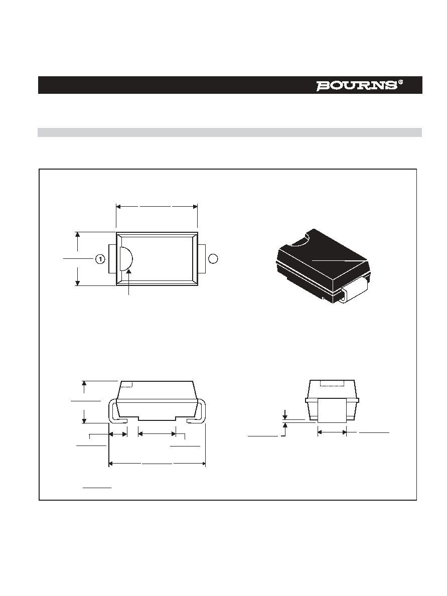
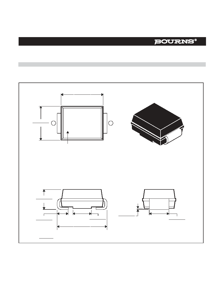
SMA (DO-214AC) Plastic Surface Mount Diode Package
This surface mount package consists of a circuit mounted on a lead frame and encapsulated within a plastic compound. The compound will
withstand soldering temperature with no deformation, and circuit performance characteristics will remain stable when operated in high
humidity conditions. Leads require no additional cleaning or processing when used in soldered assembly.
SMA
MDXXCAA
2
Index
Mark
(if needed)
2.29 - 2.92
(.090 - .115)
4.06 - 4.57
(.160 - .180)
2.00 - 2.40
(.079 - .095)
0.76 - 1.52
(.030 - .060)
4.83 - 5.59
(.190 - .220)
1.58 - 2.16
(.062 - .085)
0.10 - 0.20
(.004 - .008)
1.27 - 1.63
(.050 - .064)
DIMENSIONS ARE:
MILLIMETERS
(INCHES)
NOVEMBER 2001 - REVISED FEBRUARY 2005
Specifications are subject to change without notice.
Customers should verify actual device performance in their specific applications.
TISP43xxMMAJ/BJ Overvoltage Protector Series
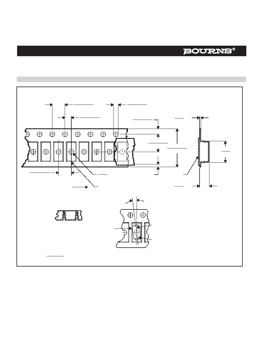
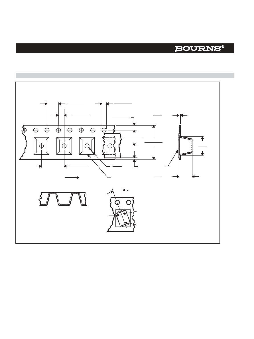
Tape Dimensions
MECHANICAL DATA
MDXXCGA
SMA Package Single-Sprocket Tape
Carrier Tape
Embossment
Direction of Feed
Maximum component
rotation
Typical component
cavity center line
Typical component
center line
Index
Mark
(If needed)
Cover
Tape
20
∞
3.90 - 4.10
(.154 - .161)
11.70 - 12.30
(.461 - .484)
5.45 - 5.55
(.215 - .219)
1.5
(.059)
MIN.
0 MIN.
4.50
(.177)
MAX.
8.20
(.323)
MAX.
0.40
(.016)
MAX.
1.65 - 1.85
(.065 - .073)
1.55 - 1.65
(.061 - .065)
1.95 - 2.05
(.077 - .081)
3.90 - 4.10
(.154 - .161)
NOTES: A. The clearance between the component and the cavity must be within 0.05 mm (.002 in) MIN. to 0.65 mm (.026 in)
MAX. so that the component cannot rotate more than 20∞ within the determined cavity.
B. Taped devices are supplied on a reel of the following dimensions:
Reel diameter: 330
mm
± 3.0 mm (12.99 in ± .12 in)
Reel hub diameter: 75 mm (2.95 in) MIN.
Reel axial hole:
13.0 mm ± 0.5 mm (.51 in ± .02 in)
C. 5000 devices per reel.
DIMENSIONS ARE:
MILLIMETERS
(INCHES)
NOVEMBER 2001 - REVISED FEBRUARY 2005
Specifications are subject to change without notice.
Customers should verify actual device performance in their specific applications.
MECHANICAL DATA
TISP43xxMMAJ/BJ Overvoltage Protector Series
SMB (DO-214AA) Plastic Surface Mount Diode Package
This surface mount package consists of a circuit mounted on a lead frame and encapsulated within a plastic compound. The compound will
withstand soldering temperature with no deformation, and circuit performance characteristics will remain stable when operated in high
humidity conditions. Leads require no additional cleaning or processing when used in soldered assembly.
SMB
MDXXBHAB
2. 00 - 2.40
(.079 - .094)
2
1
Index
Mark
(if needed)
0. 10 - 0. 20
(.004 - .008)
5. 21 - 5.59
(.205 - .220)
1. 96 - 2. 32
(.077 - .091)
3. 30 - 3. 94
(.130 - .155)
4.06 - 4.57
(.160 - .180)
0. 76 - 1.52
(.030 - .060)
1. 90 - 2.10
(.075 - .083)
DIMENSIONS ARE:
MILLIMETERS
(INCHES)
NOVEMBER 2001 - REVISED FEBRUARY 2005
Specifications are subject to change without notice.
Customers should verify actual device performance in their specific applications.
MECHANICAL DATA
TISP43xxMMAJ/BJ Overvoltage Protector Series
Tape Dimensions
SMB Package Single-Sprocket Tape
NOTES: A. The clearance between the component and the cavity must be within 0.05 mm (.002 in) MIN. to 0.65 mm (.026 in)
MAX. so that the component cannot rotate more than 20∞ within the determined cavity.
B. Taped devices are supplied on a reel of the following dimensions:
Reel diameter: 330
mm
± 3.0 mm (12.99 in ± .118 in)
Reel hub diameter: 75 mm (2.95 in) MIN.
Reel axial hole:
13.0 mm ± 0.5 mm (.512 in ± .020 in)
C. 3000 devices are on a reel.
MDXXBJA
Direction of Feed
0 MIN .
Carrier Tape
Embossment
Cover
Tape
20 ∞
Typical component
cavity center line
Maximium component
rotation
Typical component
center line
Index
Mark
(if needed)
3. 90 - 4.10
(.154 - .161 )
1. 95 - 2.05
(.077 - .081)
1. 55 - 1.65
(.061 - .065 )
MAX .
0. 40
(.016)
MAX .
4. 5
(.177)
MAX .
8. 20
(.323)
11.70 - 12.30
(.461 - .484 )
5. 45 - 5.55
(.215 - .219 )
MIN .
1. 5
(.059)
1. 65 - 1.85
(.065 - .073 )
7. 90 - 8.10
(.311 - .319 )
"TISP" is a trademark of Bourns, Ltd., a Bourns Company, and is Registered in U.S. Patent and Trademark Office.
"Bourns" is a registered trademark of Bourns, Inc. in the U.S. and other countries.