APRIL 2001 - REVISED FEBRUARY 2005
Specifications are subject to change without notice.
Customers should verify actual device performance in their specific applications.
TISP4500H3BJ Overvoltage Protector
TISP4500H3BJ
BIDIRECTIONAL THYRISTOR OVERVOLTAGE PROTECTORS
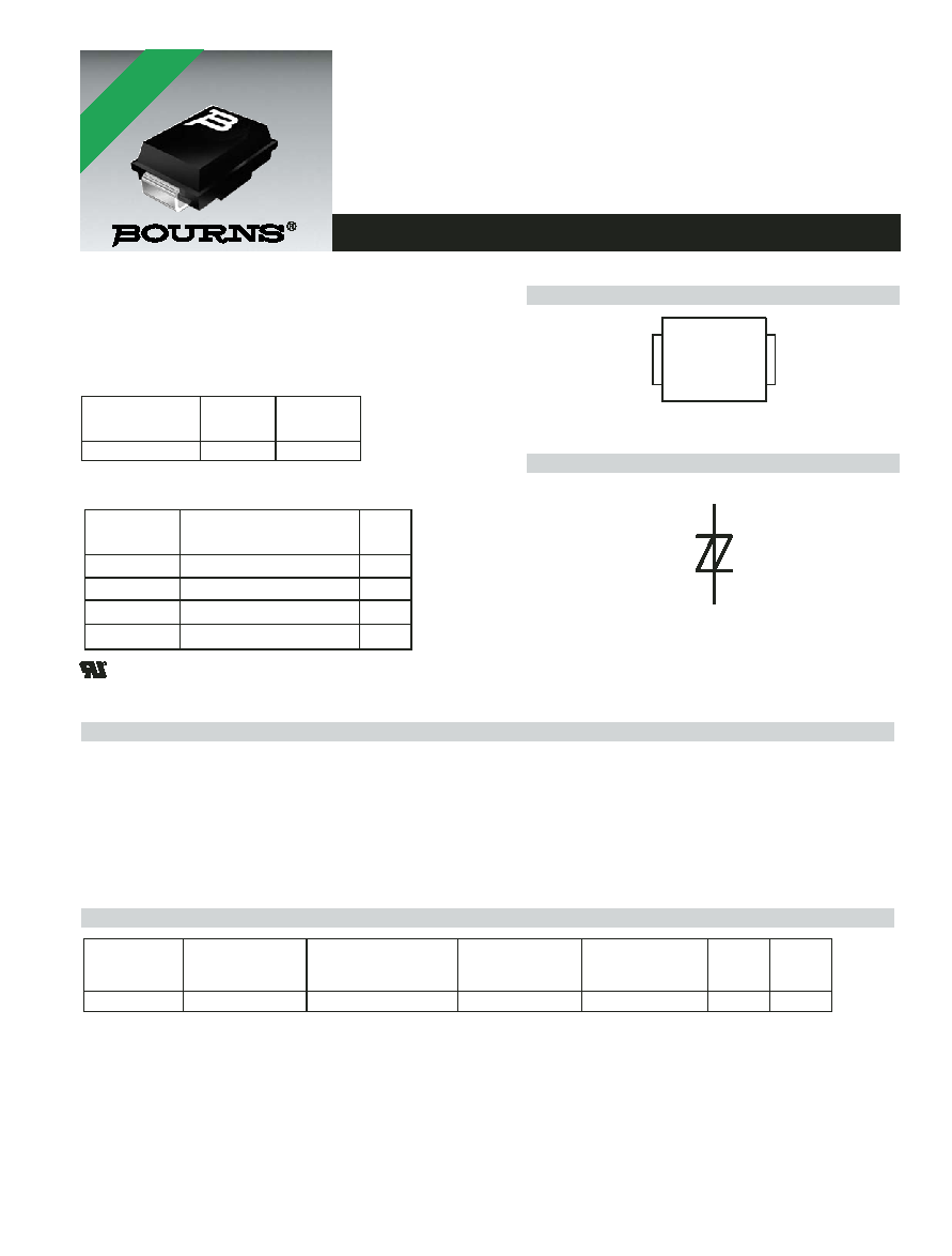
Device Symbol
Non-Conductive During K.20/21/45 Power Contact Test
- Off-State Voltage ................................................... >245 V rms
- For Controlled Environment ............................... 0 ∞C to 70 ∞C
Ion-Implanted Breakdown Region
Precise and Stable Voltage
Low Voltage Overshoot under Surge
Rated for International Surge Wave Shapes
How To Order
SMBJ Package (Top View)
Description
This device is designed to limit overvoltages on the telephone line to ±500 V over the temperature range. The minimum off-state voltage of
±350 V allows a.c. power contact voltages of up to 245 V rms to occur without clipping. The combination of these two voltages gives
protection for components having ratings of 500 V or above and ensures the protector is non-conducting for the ITU-T recommendations
K.20/21/45 230 V rms power cross test condition (test number 2.3.1).
The protector consists of a symmetrical voltage-triggered bidirectional thyristor. Overvoltages are initially clipped by breakdown clamping until
the voltage rises to the breakover level, which causes the device to crowbar into a low-voltage on state. This low-voltage on state causes the
current resulting from the overvoltage to be safely diverted through the device. The high crowbar holding current prevents d.c. latchup as the
diverted current subsides.
Device
V
DRM
V @ 0
∞
C
V
(BO)
V @ 70
∞
C
TISP4500H3BJ
350
500
.............................................. UL Recognized Component
Wave Shape
Standard
I
PPSM
A
2/10
GR-1089-CORE
500
10/250
GR-1089-CORE
230
10/700
ITU-T K.20/21/45
200
10/1000
GR-1089-CORE
100
T
R
MD-SMB-004-a
2
1
T
R
SD-TISP4xxx-001-a
*RoHS Directive 2002/95/EC Jan 27 2003 including Annex
Device
Package
Carrier
TISP4500H3BJ
SMB (DO-214AA)
Embossed Tape Reeled
TISP4500H3BJR
TISP4500H3BJR-S
Marking
Code
4500H3
Std. Qty.
3000
For Standard
Termination Finish
Order As
For Lead Free
Termination Finish
Order As
*RoHS COMPLIANT
VERSIONS
AVAILABLE
APRIL 2001 - REVISED FEBRUARY 2005
Specifications are subject to change without notice.
Customers should verify actual device performance in their specific applications.
Electrical Characteristics, 0 ∞C TA 70 ∞C (Unless Otherwise Noted)
TISP4500H3BJ Overvoltage Protector
Absolute Maximum Ratings, 0 ∞C TA 70 ∞C (Unless Otherwise Noted)
Thermal Characteristics
Parameter
Test Conditions
Min
Typ
Max
Unit
I
DRM
Repetitive peak off-
state current
V
D
= V
DRM
T
A
= 25
∞
C
T
A
= 70
∞
C
±
5
±
10
µ
A
V
(BO)
Breakover voltage
dv/dt =
±
250 V/ms,
R
SOURCE
= 300
±
500
V
V
(BO)
Impulse breakover
voltage
ITU-T recommendation K.44 (02/2000)
Figure A.3-1/K.44 10/700 impulse generator
Charge Voltage =
±
4 kV
±
500
V
I
(BO)
Breakover current
dv/dt =
±
250 V/ms,
R
SOURCE
= 300
±
0.6
A
I
H
Holding current
I
T
=
±
5 A, di/dt = -/+30 mA/ms
±
0.15
A
I
D
Off-state current
V
D
=
±
50 V
T
A
= 70
∞
C
±
10
µ
A
C
off
Off-state capacitance
f = 1 MHz, Vd = 1 V rms, V
D
= 0
f = 1 MHz, Vd = 1 V rms, V
D
= -1 V
f = 1 MHz, Vd = 1 V rms, V
D
= -2 V
f = 1 MHz, Vd = 1 V rms, V
D
= -50 V
84
67
62
31
pF
Parameter
Test Conditions
Min
Typ
Max
Unit
R
JA
Junction to free air thermal resistance
EIA/JESD51-3 PCB, I
T
= I
TSM(1000)
,
T
A
= 25
∞
C, (see Note 5)
113
∞
C/W
265 mm x 210 mm populated line card,
4-layer PCB, I
T
= I
TSM(1000)
, T
A
= 25
∞
C
50
NOTE 5: EIA/JESD51-2 environment and PCB has standard footprint dimensions connected with 5 A rated printed wiring track widths.
Rating
Symbol
Value
Unit
Repetitive peak off-state voltage
V
DRM
±350
V
Non-repetitive peak on-state pulse current (see Notes 1 and 2)
I
PPSM
500
230
200
100
A
2/10 (Telcordia GR-1089-CORE, 2/10 µs voltage wave shape)
10/250 (Telcordia GR-1089-CORE, 10/250 µs voltage wave shape)
10/700 (ITU-T K.20/21/45, 5/310 µs current wave shape)
10/1000 (Telcordia GR-1089-CORE, 10/1000 µs voltage wave shape)
T
A
= 25 ∞C
T
A
= 25 ∞C
T
A
= 25 ∞C
Non-repetitive peak on-state current (see Notes 1, 2 and 3)
I
TSM
±55
±2.0
A
50 Hz, 20 ms (1 cycle)
50 Hz, 1000 s
Junction temperature
T
J
-40 to +150
∞C
Storage temperature range
T
stg
-65 to +150
∞C
NOTES: 1. Initially the device must be in thermal equilibrium.
2. The surge may be repeated after the device returns to its initial conditions.
3. EIA/JESD51-2 environment and EIA/JESD51-3 PCB with standard footprint dimensions connected with 5 A rated printed wiring
track widths.
APRIL 2001 - REVISED FEBRUARY 2005
Specifications are subject to change without notice.
Customers should verify actual device performance in their specific applications.
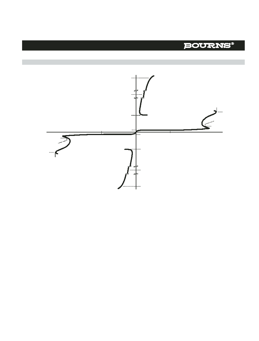
Parameter Measurement Information
TISP4500H3BJ Overvoltage Protector
Figure 1. Voltage-current Characteristic for T and R Terminals
All Measurements are Referenced to the R Terminal
-v
I
(BR)
V
(BR)
V
D
I
H
I
TSM
I
PPSM
V
(BO)
I
(BO)
I
D
Quadrant I
Switching
Characteristic
+v
+i
V
(BO)
I
(BO)
I
(BR)
V
(BR)
V
D
I
D
I
H
I
TSM
I
PPSM
-i
Quadrant III
Switching
Characteristic
PM4XAD
APRIL 2001 - REVISED FEBRUARY 2005
Specifications are subject to change without notice.
Customers should verify actual device performance in their specific applications.
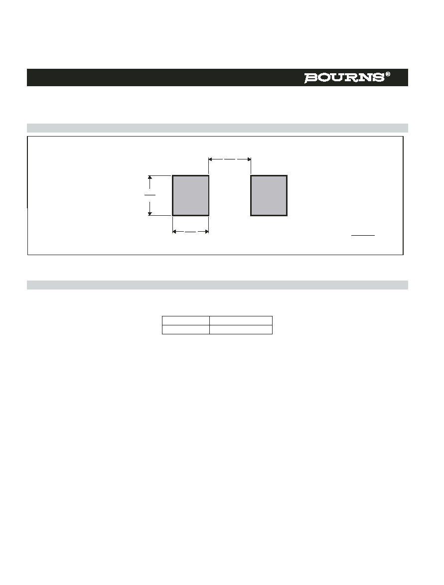
MECHANICAL DATA
TISP4500H3BJ Overvoltage Protector
Recommended Printed Wiring Land Pattern Dimensions
Device Symbolization Code
Devices will be coded as below. As the device parameters are symmetrical, terminal 1 is not identified.
SMB Land Pattern
MDXXBIB
2.54
(.100)
2.40
(.094)
2.16
(.085)
MM
(INCHES)
DIMENSIONS ARE:
Device
Symbolization Code
TISP4500H3BJ
4500H3
APRIL 2001 - REVISED FEBRUARY 2005
Specifications are subject to change without notice.
Customers should verify actual device performance in their specific applications.
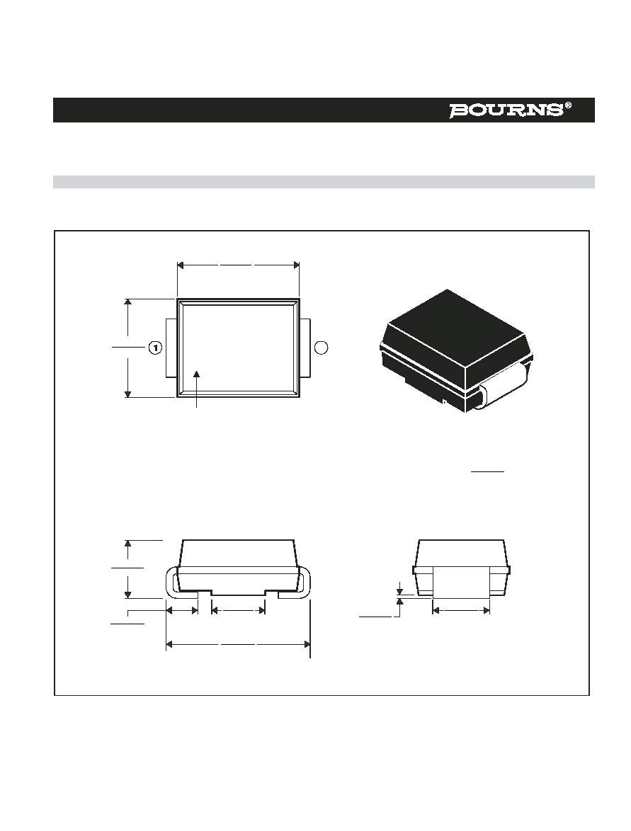
This surface mount package consists of a circuit mounted on a lead frame and encapsulated within a plastic compound. The compound will
withstand soldering temperature with no deformation, and circuit performance characteristics will remain stable when operated in high
humidity conditions. Leads require no additional cleaning or processing when used in soldered assembly.
SMBJ (DO-214AA) Plastic Surface Mount Diode Package
TISP4500H3BJ Overvoltage Protector
MECHANICAL DATA
SMB
MDXXBHAB
2
Index
Mark
(if needed)
MM
(INCHES)
DIMENSIONS ARE:
4.06 - 4.57
(.160 - .180)
3.30 - 3.94
(.130 - .155)
1.96 - 2.32
(.077 - .091)
0.10 - 0.20
(.004 - .008)
0.76 - 1.52
(.030 - .060)
2.00 - 2.40
(.079 - .094)
1.90 - 2.10
(.075 - .083)
5.21 - 5.59
(.205 - .220)
APRIL 2001 - REVISED FEBRUARY 2005
Specifications are subject to change without notice.
Customers should verify actual device performance in their specific applications.
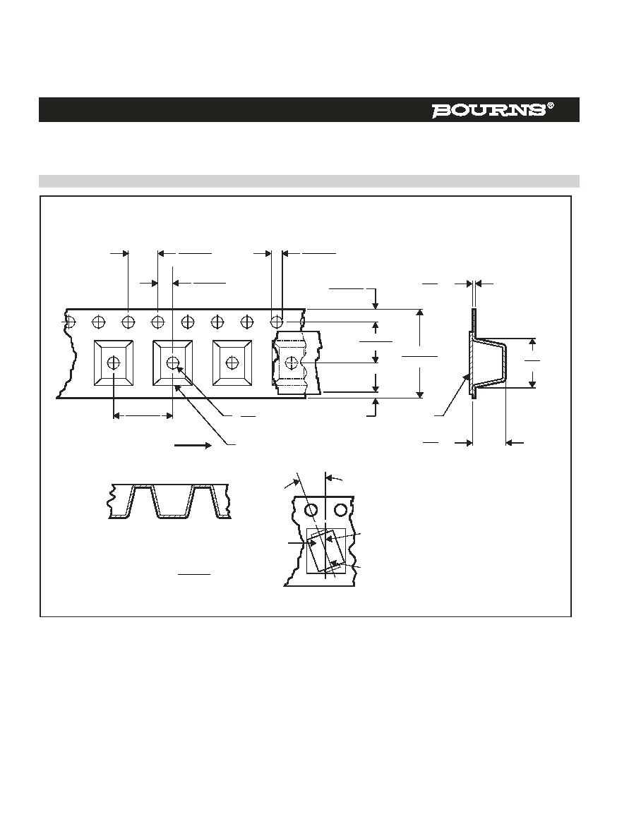
MECHANICAL DATA
TISP4500H3BJ Overvoltage Protector
Tape DImensions
SMB Package Single-Sprocket Tape
Direction of Feed
Embossment
Carrier Tape
Cover
Tape
NOTES: A. The clearance between the component and the cavity must be within 0.05 mm (.002 in.)
(.026 in.)
MIN. to 0.65 mm
MAX. so that the
compon n
e t cannot rotate more than 20
∞
within the determined cavity.
B. Taped devices are supplied on a reel of the following dimensions:-
Reel diameter:
330
±
3.0 mm
(2.95 in.)
(.512
±
.020 in.)
(12.99
±
.118 in.)
Reel hub diameter: 75 mm
MIN.
Reel axial hole:
13.0
±
0.5 mm
C. 3000 devices are on a reel.
MDXXBJA
20
∞
Typical component
cavity cent r
e line
Maximium component
rotation
Typical component
cent r
e line
Index
Mark
3.90 - 4.10
(.154 - .161)
1.95 - 2.05
(.077 - .081)
1.55 - 1.65
(.061 - .065)
1.65 - 1.85
(.065 - .073)
5.54 - 5.55
(.215 - .219)
11.70 - 12.30
(.461 - .484)
7.90 - 8.10
(.311 - .319)
8.20
(.323)
MAX.
0.40
(.016)
MAX.
4.50
(.177)
MAX.
0 MIN.
1.50
(.059)
MIN.
ÿ
MM
(INCHES)
DIMENSIONS ARE:
"TISP" is a trademark of Bourns, Ltd., a Bourns Company, and is Registered in U.S. Patent and Trademark Office.
"Bourns" is a registered trademark of Bourns, Inc. in the U.S. and other countries.