AUGUST 2004 ≠ REVISED FEBRUARY 2005
Specifications are subject to change without notice.
Customers should verify actual device performance in their specific applications.
TISP9110LDM Overvoltage Protector
TISP9110LDM
INTEGRATED COMPLEMENTARY BUFFERED-GATE SCRS
FOR DUAL POLARITY SLIC OVERVOLTAGE PROTECTION
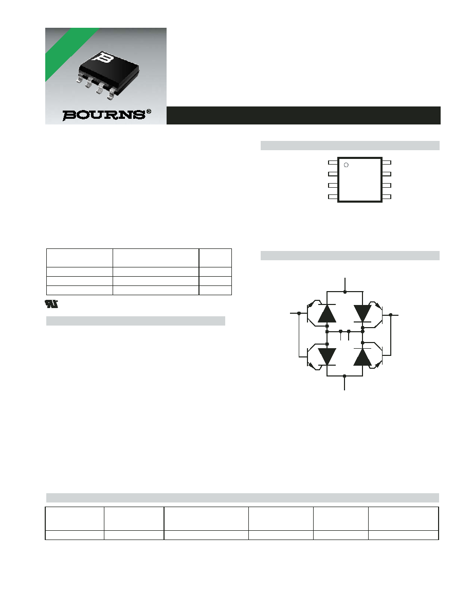
Device Symbol
High Performance Protection for SLICs with +ve and -ve
Battery Supplies
≠ Wide -110 V to +110 V Programming Range
≠ Low 5 mA max. Gate Triggering Current
≠ Dynamic Protection Performance Specified for
International Surge Waveshapes
Applications include:
≠ Wireless Local Loop
≠ Access Equipment
≠ Regenerated POTS
≠ VOIP Applications
Rated for International Surge Wave Shapes
How To Order
8-SOIC (210 mil) Package (Top View)
Description
The TISP9110LDM is a programmable overvoltage protection
device designed to protect modern dual polarity supply rail
ringing SLICs (Subscriber Line Interface Circuits) against
overvoltages on the telephone line. Overvoltages can be caused
by lightning, a.c. power contact and induction. Four separate
protection structures are used; two positive and two negative to
provide optimum protection during Metallic (Differential) and
Longitudinal (Common Mode) protection conditions in both
polarities. Dynamic protection performance is specified under
typical international surge waveforms from Telcordia GR-1089-
CORE, ITU-T K.44 and YD/T 950.
The TISP9110LDM is programmed by connecting the G1 and G2
gate terminals to the negative (-V
(BAT)
) and positive (+V
(BAT)
)
Wave Shape
Standard
I
PPSM
A
2/10
GR-1089-CORE
100
10/700
ITU-T K.20/21/45
45
10/1000
GR-1089-CORE
30
MD-8SOIC(210)-003-a
NC - No internal connection
Terminal typical application names shown in
parenthesis
1
2
3
4
5
6
7
8
NC
Ground
Ground
NC
(-V
(BAT)
) G1
(Tip or Ring) Line
(Ring or Tip) Line
(+V
(BAT)
) G2
SD-TISP9-001-a
G2
G1
Ground
Line
Line
SLIC Battery supplies respectively. This creates a protector operating at typically +1.4 V above +V
(BAT)
and -1.4 V below -V
(BAT)
under a.c.
power induction and power contact conditions. The protector gate circuitry incorporates 4 separate buffer transistors designed to provide
independent control for each protection element. The gate buffer transistors minimize supply regulation issues by reducing the gate current
drawn to around 5 mA, while the high voltage base emitter structures eliminate the need for expensive reverse bias protection gate diodes.
The TISP9110LDM is rated for common surges contained in regulatory requirements such as ITU-T K.20, K.45, Telcordia GR-1089-CORE,
YD/T 950. By the use of appropriate overcurrent protection devices such as the Bourns
Æ
Multifuse
Æ
and Telefuse
TM
devices, circuits can be
designed to comply with modern telecom standards.
*RoHS Directive 2002/95/EC Jan 27 2003 including Annex
............................................... UL Recognized Component
Device
Package
Carrier
Marking Code
Standard Quantity
TISP9110LDM
8-SOIC (210 mil)
Embossed Tape Reeled
TISP9110LDMR-S
9110L
2000
For Lead Free
Termination Finish
Order As
*R
oH
S C
OM
PL
IA
NT

AUGUST 2004 ≠ REVISED FEBRUARY 2005
Specifications are subject to change without notice.
Customers should verify actual device performance in their specific applications.
Absolute Maximum Ratings, TA = 25 ∞C (Unless Otherwise Noted)
TISP9110LDM Overvoltage Protector
Electrical Characteristics for any Section, TA = 25 ∞C (Unless Otherwise Noted)
Parameter
Test Conditions
Min
Typ
Max
Unit
I
D
Off-state current
V
D
= V
DRM
, V
G1(Line)
= 0, V
G2
+5 V
V
D
= V
DRM
, V
G2(Line)
= 0, V
G1
-5 V
T
A
= 25 ∞C
T
A
= 85 ∞C
T
A
= 25 ∞C
T
A
= 85 ∞C
-5
-50
+5
+50
µA
I
G1(Line)
Negative-gate leakage current
V
G1(Line)
= -220 V
-5
µA
I
G2(Line)
Positive-gate leakage current
V
G2(Line)
= +220 V
+5
µA
V
G1L(BO)
Gate - Line impulse breakover voltage
V
G1
= -100 V, I
T
= -100 A (see Note 6)
V
G1
= -100 V, I
T
= -30 A
2/10 µs
10/1000 µs
-15
-11
V
V
G2L(BO)
Gate - Line impulse breakover voltage
V
G2
= +100 V, I
T
= +100 A (see Note 6)
V
G2
= +100 V, I
T
= +30 A
2/10 µs
10/1000 µs
+15
+11
V
I
H
-
Negative holding current
V
G1
= -60 V, I
T
= -1 A, di/dt = 1 A/ms
-150
mA
I
G1T
Negative-gate trigger current
I
T
= -5 A, t
p(g)
20 µs, V
G1
= -60 V
+5
mA
I
G2T
Positive-gate trigger current
I
T
= 5 A, t
p(g)
20 µs, V
G2
= 60 V
-5
mA
C
O
Line - Ground off-state capacitance
f = 1 MHz, V
D
= -3 V, G1 & G2 open circuit
32
pF
NOTE:
6. Voltage measurements should be made with an oscilloscope with limited bandwidth (20 MHz) to avoid high frequency noise.
Rating
Symbol
Value
Unit
Repetitive peak off-state voltage
V
G1(Line)
= 0, V
G2
+5 V
V
G2(Line)
= 0, V
G1
-5 V
V
DRM
-120
+120
V
Non-repetitive peak impulse current (see Notes 1, 2, 3 and 4)
I
PPSM
±100
±45
±30
A
2/10 µs (Telcordia GR-1089-CORE)
5/310 µs (ITU-T K.20, K.21 & K.45, K.44 open-circuit voltage wave shape 10/700 µs)
10/1000 µs (Telcordia GR-1089-CORE)
Non-repetitive peak on-state current, 50 Hz / 60 Hz (see Notes 1, 2, 3 and 5)
I
TSM
9.0
5.0
1.7
A
0.2 s
1 s
900 s
Maximum negative battery supply voltage
V
G1M
-110
V
Maximum positive battery supply voltage
V
G2M
+110
V
Maximum differential battery supply voltage
V
(BAT)M
220
V
Junction temperature
T
J
-40 to +150
∞C
Storage temperature range
T
stg
-65 to +150
∞C
NOTES: 1. Initially the device must be in thermal equilibrium with T
J
= 25 ∞C. The surge may be repeated after the device returns to its initial
conditions.
2. The rated current values may be applied to either of the Line to Ground terminal pairs. Additionally, both terminal pairs may have
their rated current values applied simultaneously (in this case the Ground terminal current will be twice the rated current value of a
single terminal pair).
3. Rated currents only apply if pins 6 & 7 (Ground) are connected together.
4. Applies for the following bias conditions: V
G1
= -20 V to -110 V, V
G2
= 0 V to +110 V.
5. EIA/JESD51-2 environment and EIA/JESD51-7 high effective thermal conductivity test board (multi-layer) connected with 0.6 mm
printed wiring track widths.
AUGUST 2004 ≠ REVISED FEBRUARY 2005
Specifications are subject to change without notice.
Customers should verify actual device performance in their specific applications.
Thermal Characteristics, TA = 25 ∞C (Unless Otherwise Noted)
Parameter Measurement Information
TISP9110LDM Overvoltage Protector
Parameter
Test Conditions
Min Typ Max
Unit
R
JA
Junction to ambient thermal resistance
EIA/JESD51-7 PCB, EIA/JESD51-2 Environment, P
TOT
= 4 W
(See Note 7)
55
∞C/W
NOTE
7. EIA/JESD51-7 high effective thermal conductivity test board (multi-layer) connected with 0.6 mm printed wiring track widths.
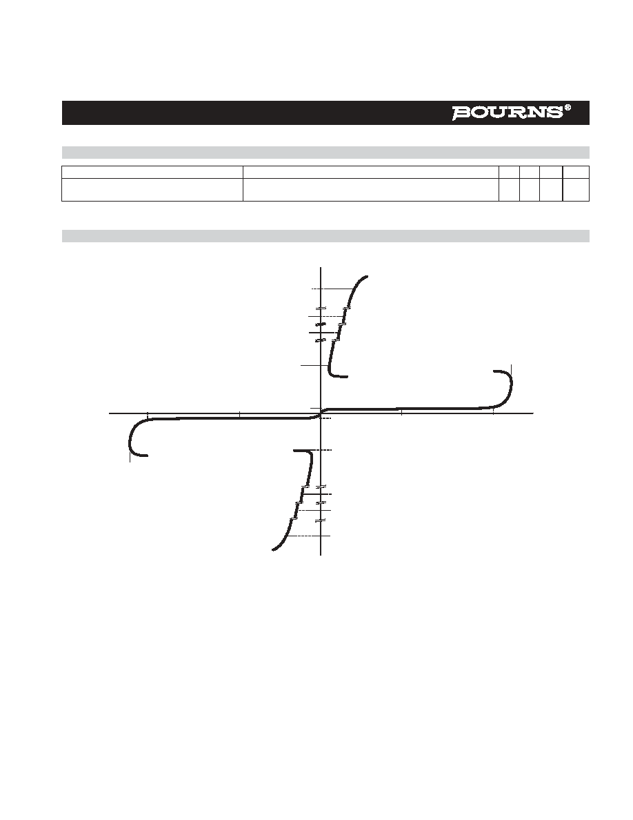
Figure 1. Voltage-Current Characteristic
Unless Otherwise Noted, All Voltages are Referenced to the Ground Terminal
Quadrant III
Switching
Characteristic
-v
V
G1
V
D
I
H
I
TRM
I
PPSM
V
(BO)
+i
-i
I
D
PM-TISP9-001-a
I
TSM
V
G2
V
D
V
(BO)
I
H
I
TRM
I
PPSM
Quadrant I
Switching
Characteristic
I
D
+v
I
TSM
AUGUST 2004 ≠ REVISED FEBRUARY 2005
Specifications are subject to change without notice.
Customers should verify actual device performance in their specific applications.
Typical Characteristics
TISP9110LDM Overvoltage Protector
Figure 2.
Figure 3.
OFF-STATE CAPACITANCE
vs
OFF-STATE VOLTAG E
V
D
- Off-state Voltage - V
0.1
1
10
100
C
o
-
Of
f-s
ta
te
Cap
aci
ta
nc
e -
pF
10
15
20
30
35
40
45
25
50
TC-TISP9-001-a
T
J
= 25 ∞C
V
d
= 1 Vrms
NON-REPETITIVE PEAK ON-STATE CURRENT
vs
CURRENT DURATION
t - Current Duration - s
0.1
1
10
100
1000
I
TS
M(t
)
-
Non
-
R
e
p
e
t
it
i
v
e
Peak
On
-Sta
te
Curre
n
t
-
A
1.5
2
3
4
5
6
7
8
9
15
1
10
TI-TISP9-001-a
V
GEN
= 600 Vrms, 50/60 Hz
R
GEN
= 1.4*V
GEN
/I
TSM(t)
EIA/JESD51-2 ENVIRONMENT
EIA/JESD51-7 PCB, T
A
= 25 ∞C
SIMULTANEOUS OPERATION
OF R AND T TERMINALS.
GROUND TERMINAL
CURRENT = 2 x I
TSM(t)
Thermal Information
AUGUST 2004 ≠ REVISED FEBRUARY 2005
Specifications are subject to change without notice.
Customers should verify actual device performance in their specific applications.
TISP9110LDM Overvoltage Protector
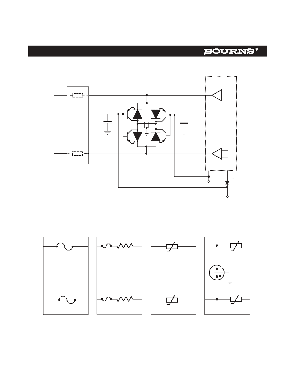
APPLICATIONS INFORMATION
SLIC
-V
BAT
SLIC
PROTECTOR
TISP9110LDM
C1
220 nF
Tip
Ring
D1
C2
220 nF
+V
BAT
Overcurrent
Protection
Figure 4. Typical Application Diagram
AI-TISP9-001-a
GR-1089-Core Intra Building
Overcurrent Protection 1
F1b
B0500T
F1a
B0500T
ITU-T K20 (Basic)
Overcurrent Protection 3
MF-SM013-250
+ t∞
MF-SM013-250
+ t∞
GR-1089-CORE
Overcurrent Protection 2
Telcordia
GR-1089-CORE Issue 3
compliant LFR (Custom)
ITU-T K20 (Enhanced)
Overcurrent Protection 4
35 CPTC
+ t∞
+ t∞
35
CPTC
* 2027-35
GDT (Bourns)
* Agreed Primary
Figure 5. Typical Overcurrent Protection
"TISP" is a trademark of Bourns, Ltd., a Bourns Company, and is Registered in U.S. Patent and Trademark Office.
"Bourns" is a registered trademark of Bourns, Inc. in the U.S. and other countries.