Revision 2.2
April 2001
1
BSI
Ultra Low Power/Voltage CMOS SRAM
1M x 16 or 2M x 8 bit switchable
The BS616UV1620 is a high performance, ultra low power CMOS Static
Random Access Memory organized as 1,048,676 words by 16 bits or
2,097,152 bytes by 8 bits selectable by CIO pin and operates in a wide
range of 1.8V to 2.3V supply voltage.
Advanced CMOS technology and circuit techniques provide both high
speed and low power features with a typical CMOS standby current
of 1.2uA and maximum access time of 70/100ns in 2.0V operation.
This device provide three control inputs and three states output drivers
for easy memory expansion.
The BS616UV1620 has an automatic power down feature, reducing the
power consumption significantly when chip is deselected.
The BS616UV1620 is available in DICE form and 48-pin BGA type.
POWER DISSIPATION
SPEED
(ns)
STANDBY
(I
CCSB1
, Max)
Operating
(I
CC
, Max)
PRODUCT
FAMILY
OPERATING
TEMPERATURE
Vcc RANGE
Vcc=2.0V
Vcc=2.0V
Vcc=2.0V
PKG TYPE
BS616UV1620BC
BGA-48-0810
BS616UV1620FC
+0
O
C to +70
O
C
1.8V ~ 2.3V
70 / 100
30uA
25mA
BGA-48-0912
BS616UV1620BI
BGA-48-0810
BS616UV1620FI
-40
O
C to +85
O
C
1.8V ~ 2.3V
70 / 100
40uA
30mA
BGA-48-0912
� Ultra low operation voltage : 1.8 ~ 2.3V
� Ultra low power consumption :
Vcc = 1.8V C-grade : 25mA (Max.) operating current
I- grade : 30mA (Max.) operating current
1.2uA (Typ.) CMOS standby current
� High speed access time :
-70 70ns (Max.) at Vcc = 2.0V
-10 100ns (Max.) at Vcc = 2.0V
� Automatic power down when chip is deselected
� Three state outputs and TTL compatible
� Fully static operation
� Data retention supply voltage as low as 1.5V
� Easy expansion with CE1, CE2 and OE options
� I/O Configuration x8/x16 selectable by CIO, LB and UB pin
DESCRIPTION
FEATURES
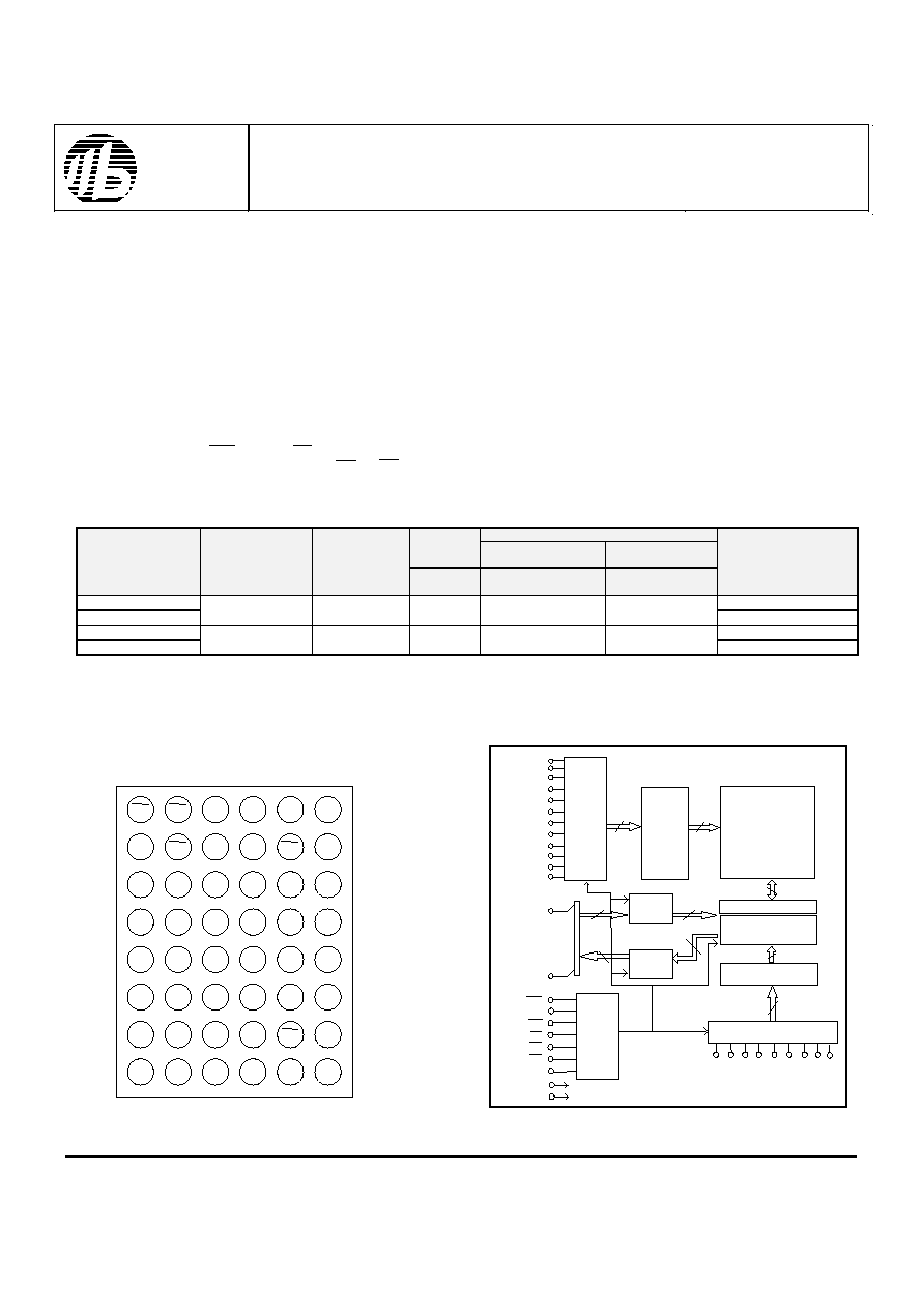
BLOCK DIAGRAM
PRODUCT FAMILY
Brilliance Semiconductor Inc
. reserves the right to modify document contents without notice.
PIN CONFIGURATIONS
R0201-BS616UV1620
LB
OE
A0
A1
A2
CE2
D8
UB
A3
A4
CE1
D0
D9
D10
A5
A6
D1
D2
VSS
D11
A17
A7
D3
VCC
VCC
D12
A16
D4
VSS
D14
D13
A14
A15
D5
D6
D15
CIO
.
A12
A13
WE
D7
A18
A8
A9
A10
A11
SAE.
A
B
C
D
E
F
G
H
1
2
3
4
5
6
A19
Row
Decoder
Memory Array
4096 x 4096
Column I/O
Write Driver
Sense Amp
Column Decoder
Data
Buffer
Output
A1 A2 A3
Data
Input
Buffer
Control
Vss
Vdd
OE
WE
D0
A8
A12
16(8)
16(8)
16(8)
16(8)
CE1
D15
A11
A7
A17
A13
16(18)
256(512)
4096
4096
24
A10
A9
A0
A6
A4
A16
A14
Address
Input
Buffer
A18
Address Input Buffer
.
.
.
.
UB
.
.
.
.
LB
A15
CIO
CE2
(SAE)
A5
A19
BS616UV1620
48-Ball CSP top View
Revision 2.2
April 2001
2
Name
Function
A0-A19 Address Input
These 20 address inputs select one of the 1,048,576 x 16-bit words in the RAM.
SAE Address Input
This address input incorporates with the above 20 address inputs select one of the
2,097,152 x 8-bit bytes in the RAM if the CIO is LOW. Don't use when CIO is HIGH.
CIO x8/x16 select input
This input selects the organization of the SRAM. 1,048,576 x 16-bit words
configuration is selected if CIO is HIGH. 2,097,152 x 8-bit bytes configuration is
selected if CIO is LOW.
CE1 Chip Enable 1 Input
CE2 Chip Enable 2 Input
CE1 is active LOW and CE2 is active HIGH. Both chip enables must be active when
data read from or write to the device. If either chip enable is not active, the device is
deselected and is in a standby power mode. The DQ pins will be in the high
impedance state when the device is deselected.
WE Write Enable Input
The write enable input is active LOW and controls read and write operations. With the
chip selected, when WE is HIGH and OE is LOW, output data will be present on the
DQ pins; when WE is LOW, the data present on the DQ pins will be written into the
selected memory location.
OE Output Enable Input
The output enable input is active LOW. If the output enable is active while the chip is
selected and the write enable is inactive, data will be present on the DQ pins and they
will be enabled. The DQ pins will be in the high impedance state when OE is inactive.
LB and UB Data Byte Control Input
Lower byte and upper byte data input/output control pins. The chip is deselected when
both LB and UB pins are HIGH.
D0 - D15 Data Input/Output Ports
These 16 bi-directional ports are used to read data from or write data into the RAM.
Vcc
Power Supply
Gnd
Ground
PIN DESCRIPTIONS
BSI
BS616UV1620
R0201-BS616UV1620
Revision 2.2
April 2001
3
MODE CE1
CE2
OE
WE
CIO
LB
UB
SAE
D0~7
D8~15
VCC
Current
H X
X X
Fully Standby
X L
X X X
X X
X High-Z
High-Z I
CCSB
, I
CCSB1
Output
Disable
L H H H X X X X High-Z
High-Z
I
CC
L H
Dout High-Z
H L
High-Z Dout
Read from SRAM
( WORD mode )
L H L H H
L L
X
Dout Dout
I
CC
L H
Din
X
H L
X
Din
Write to SRAM
( WORD mode )
L H X L H
L L
X
Din Din
I
CC
Read from SRAM
( BYTE Mode )
L H L H L X X A-1 Dout High-Z
I
CC
Write to SRAM
( BYTE Mode )
L H X L L X X A-1 Din
X
I
CC
TRUTH TABLE
BSI
BS616UV1620
C
IN
Input
Capacitance
V
IN
=0V
6
pF
C
DQ
Input/Output
Capacitance
V
I/O
=0V
8
pF
RANGE
AMBIENT
TEMPERATURE
Vcc
Commercial
0
O
C to +70
O
C
1.8V ~ 2.3V
Industrial
-40
O
C to +85
O
C
1.8V ~ 2.3V
ABSOLUTE MAXIMUM RATINGS
(1)
OPERATING RANGE
CAPACITANCE
(1)
(TA = 25
o
C, f = 1.0 MHz)
1. Stresses greater than those listed under ABSOLUTE MAXIMUM
RATINGS may cause permanent damage to the device. This is a
stress rating only and functional operation of the device at these
or any other conditions above those indicated in the operational
sections of this specification is not implied. Exposure to absolute
maximum rating conditions for extended periods may affect
reliability.
1. This parameter is guaranteed and not tested.
SYMBOL
PARAMETER
RATING
UNITS
V
TERM
Terminal Voltage with
Respect to GND
-0.5 to
Vcc+0.5
V
T
BIAS
Temperature Under Bias
-40 to +125
O
C
T
STG
Storage Temperature
-60 to +150
O
C
P
T
Power Dissipation
1.0
W
I
OUT
DC Output Current
20
mA
R0201-BS616UV1620
PAR
SYMBOL
AMETER
CONDITIONS
MAX.
UNIT
Revision 2.2
April 2001
4
PARAMETER
NAME
PARAMETER
TEST CONDITIONS
MIN. TYP.
(1)
MAX.
UNITS
V
IL
Guaranteed Input Low
Voltage
(2)
Vcc= 2.0V
-0.5
--
0.4
V
V
IH
Guaranteed Input High
Voltage
(2)
Vcc= 2.0V
1.4
--
Vcc+0.2
V
I
IL
Input Leakage Current
Vcc = Max, V
IN
= 0V to Vcc
--
--
1
uA
I
OL
Output Leakage Current
Vcc = Max, CE1 = V
OE = V , V = 0V to
IH
, or CE2 = V
iL
, or
IH
I/O
Vcc
--
--
1
uA
V
OL
Output Low Voltage
= 1mA
Vcc= max, I
OL
Vcc= 2.0V
--
--
0.4
V
V
OH
Output High Voltage
= -0.5mA
Vcc= Min, I
OH
Vcc= 2.0V
1.6
--
--
V
I
CC
Operating Power Supply
Current
Vcc= max, CE1 = V
V
IH
,
I = 0mA, F = Fmax
IL
and CE2 =
DQ
(3)
Vcc= 2.0V
--
--
25
mA
I
CCSB
Standby Current-TTL
Vcc= max, CE1 = V
V , I = 0mA
IH
or CE2 =
IL
DQ
Vcc= 2.0V
--
--
0.8
mA
I
CCSB1
Standby Current-CMOS
Vcc= max,CE1
Vcc-0.2V
CE2
0.2V, or LB and UB
Vcc - 0.2V,
, or
V
IN
Vcc - 0.2V or V
IN
0.2V
Vcc= 2.0V
--
1.2
30
uA
1. Typical characteristics are at TA = 25
o
C.
2. These are absolute values with respect to device ground and all overshoots due to system or tester notice are included.
3. Fmax = 1/ t
RC
.
DC ELECTRICAL CHARACTERISTICS
( TA = 0
o
C to + 70
o
C )
BSI
BS616UV1620
R0201-BS616UV1620
Revision 2.2
April 2001
5
SYMBOL
PARAMETER
TEST CONDITIONS
MIN. TYP.
(1)
MAX.
UNITS
V
DR
Vcc for Data Retention
CE1
Vcc - 0.2V or CE2
0.2V or
LB
Vcc - 0.2V and UB
Vcc - 0.2V
V
IN
Vcc - 0.2V or V
IN
0.2V
1.5
--
--
V
I
CCDR
Data Retention Current
CE1
Vcc - 0.2V or CE2
0.2V
V
IN
Vcc - 0.2V or V
IN
0.2V
--
0.8
15
uA
t
CDR
Chip Deselect to Data
Retention Time
0
--
--
ns
t
R
Operation Recovery Time
See Retention Waveform
T
RC
(2)
--
--
ns
DATA RETENTION CHARACTERISTICS
( TA = 0
o
C to +70
o
C )
1. Vcc = 1.5V, T
A
= + 25
O
C
2. t
RC
= Read Cycle Time
BSI
BS616UV1620
LOW V
CC
DATA RETENTION WAVEFORM (1)
( CE1 Controlled )
CE1
Data Retention Mode
Vcc
t
CDR
Vcc
t
R
V
IH
V
IH
Vcc
V
DR
1.5V
CE1
Vcc - 0.2V
LOW V
CC
DATA RETENTION WAVEFORM (2)
( CE2 Controlled )
CE2
Data Retention Mode
Vcc
t
CDR
Vcc
t
R
V
IL
V
IL
Vcc
V
DR
1.5V
CE2
0.2V
R0201-BS616UV1620
Revision 2.2
April 2001
6
Input Pulse Levels
Input Rise and Fall Times
Input and Output
Timing Reference Level
Vcc/0V
5ns
0.5Vcc
AC ELECTRICAL CHARACTERISTICS
( TA = 0
o
C to +70
o
C, Vcc = 2.0V )
READ CYCLE
AC TEST CONDITIONS
AC TEST LOADS AND WAVEFORMS
BSI
BS616UV1620
KEY TO SWITCHING WAVEFORMS
WAVEFORM
INPUTS
OUTPUTS
MUST BE
STEADY
MAY CHANGE
FROM H TO L
DON T CARE:
ANY CHANGE
PERMITTED
DOES NOT
APPLY
MUST BE
STEADY
WILL BE
CHANGE
FROM H TO L
CHANGE :
STATE
UNKNOWN
CENTER
LINE IS HIGH
IMPEDANCE
"OFF "STATE
MAY CHANGE
FROM L TO H
WILL BE
CHANGE
FROM L TO H
,
JEDEC
PARAMETER
NAME
PARAMETER
NAME
DESCRIPTION
BS616UV1620-70
MIN. TYP. MAX.
UNIT
Data Byte Control to Output High Z
Read Cycle Time
t
AVAX
t
AVQV
t
E1LQV
t
GLQV
t
BE
t
E1HQZ
t
GHQZ
t
BDO
t
GLQX
t
E1LQX
t
BA
t
RC
t
AA
t
ACS1
t
BA
t
OE
t
CL1
t
BE
t
OLZ
t
CHZ
t
BDO
t
OHZ
t
OH
Address Access Time
Chip Select Access Time
Data Byte Control Access Time
Chip Select to Output Low Z
Output Enable to Output in Low Z
Chip Deselect to Output in High Z
Output Disable to Output in High Z
Output Disable to Output Address Change
Data Byte Control to Output Low Z
70
10
10
10
0
0
0
10
t
AXQX
ns
ns
ns
ns
ns
ns
ns
ns
ns
ns
ns
ns
Output Enable to Output Valid
(CE1)
(CE2,CE1)
70
70
70
50
50
35
30
30
BS616UV1620-10
MIN. TYP. MAX.
100
15
15
15
0
0
0
15
100
100
100
60
60
40
35
35
(CE2,CE1)
ns
t
E2LQV
t
ACS2
(CE2)
Chip Select Access Time
(LB,UB)
(LB,UB)
(LB,UB)
R0201-BS616UV1620
800
THEVENIN EQUIVALENT
ALL INPUT PULSES
10%
90%
Vcc
GND
5ns
90%
10%
1.2V
OUTPUT
FIGURE 2
2V
OUTPUT
INCLUDING
JIG AND
SCOPE
1333
2000
5PF
FIGURE 1B
2V
OUTPUT
INCLUDING
JIG AND
SCOPE
1333
100PF
FIGURE 1A
2000
Revision 2.2
April 2001
7
NOTES:
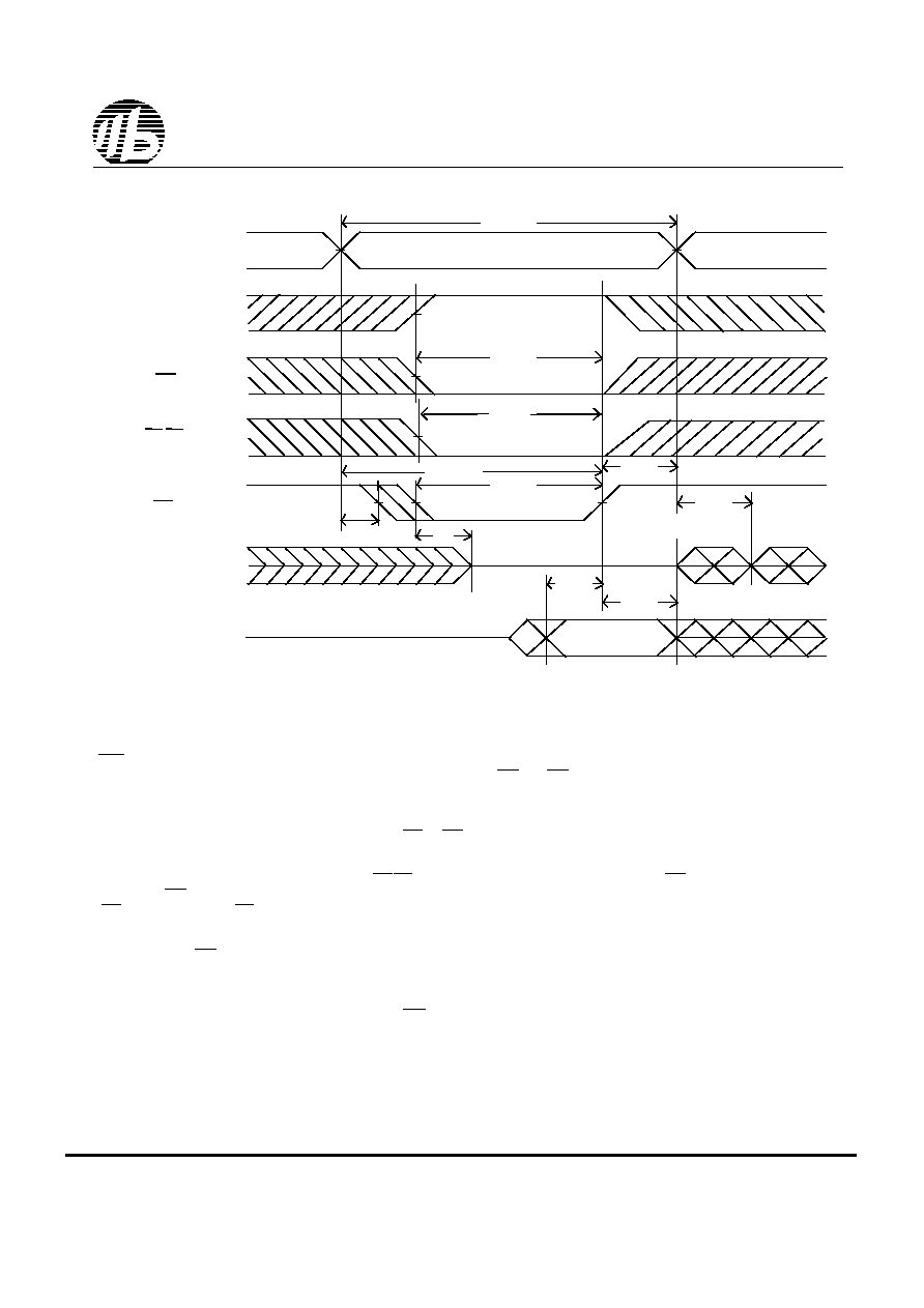
1. WE is high in read Cycle.
2. Device is continuously selected when CE1 = V
IL
and CE2 = V
IH
.
3. Address valid prior to or coincident with CE1 transition low and CE2 transition high.
4. OE = V
IL
.
5. Transition is measured 500mV from steady state with CL = 30pF as shown in Figure 1B.
The parameter is guaranteed but not 100% tested.
�
SWITCHING WAVEFORMS (READ CYCLE)
BSI
BS616UV1620
R0201-BS616UV1620
READ CYCLE3
(1,4)
READ CYCLE2
(1,3,4)
READ CYCLE1
(1,2,4)
t
RC
t
OH
t
AA
D
OUT
ADDRESS
t
OH
t
CLZ
t
CHZ
(5)
D
OUT
CE1
(5)
t
ACS1
CE2
t
OH
t
RC
t
OE
D
OUT
LB,UB
CE1
OE
ADDRESS
t
CLZ
(5)
t
ACS1
t
CHZ
(1,5)
t
OHZ
(5)
t
OLZ
t
AA
t
BDO
t
BA
t
BE
CE2
t
ACS2
t
ACS2
Revision 2.2
April 2001
8
AC ELECTRICAL CHARACTERISTICS
( TA = 0
o
C to +70
o
C, Vcc = 2.0V )
WRITE CYCLE
JEDEC
PARAMETER
NAME
PARAMETER
NAME
DESCRIPTION
BS616UV1620-70
MIN. TYP. MAX.
UNIT
Data Hold from Write Time
Write Cycle Time
t
AVAX
t
E1LWH
t
AVWL
t
WLWH
t
BW
t
DVWH
t
GHQZ
t
WHQX
t
WHDX
t
WLQZ
t
WHAX
t
AVWH
t
WC
t
CW
t
AS
t
AW
t
WP
t
WR
t
BW
t
WHZ
t
DW
t
DH
t
OHZ
t
OW
Chip Select to End of Write
Address Set up Time
Address Valid to End of Write
Write Recovery Time
Write to Output in High Z
Data to Write Time Overlap
Output Disable to Output in High Z
End of Write to Output Active
Data Byte Control to End of Write
70
70
0
70
50
0
60
0
30
0
0
5
30
30
ns
ns
(CE2, CE1, WE)
ns
ns
ns
ns
ns
ns
ns
ns
ns
ns
SWITCHING WAVEFORMS (WRITE CYCLE)
Write Pulse Width
BS616UV1620-10
MIN. TYP. MAX.
100
100
0
100
70
0
80
0
40
0
0
10
40
40
BSI
BS616UV1620
(LB,UB)
R0201-BS616UV1620
WRITE CYCLE1
(1)
t
WR
t
WC
(3)
t
CW
(11)
t
BW
(2)
t
WP
t
AW
t
OHZ
(4,10)
t
AS
(3)
t
DH
t
DW
D
IN
D
OUT
WE
CE1
OE
ADDRESS
(5)
CE2
(5)
(5)
LB,UB
Revision 2.2
April 2001
9
BSI
BS616UV1620
R0201-BS616UV1620
t
WC
t
CW
(11)
(2)
t
WP
t
AW
t
WHZ
(4,10)
t
AS
t
WR
(3)
t
DH
t
DW
D
IN
D
OUT
WE
CE1
ADDRESS
t
DH
(7)
(8)
(8,9)
CE2
LB,UB
t
BW
(5)
(5)
WRITE CYCLE2
(1,6)
NOTES:
1. WE must be high during address transitions.
2. The internal write time of the memory is defined by the overlap of CE2, CE1 and WE low.
All signals must be active to initiate a write and any one signal can terminate
a write by going inactive. The data input setup and hold timing should be referenced to the
second transition edge of the signal that terminates the write.
3. T
WR
is measured from the earlier of CE2 going low, or CE1 or WE going high at the end of write cycle.
4. During this period, DQ pins are in the output state so that the input signals of opposite
phase to the outputs must not be applied.
5. If the CE2 high transition or CE1 low transition or LB,UB low transition occurs simultaneously with the WE low transitions
or after the WE transition, output remain in a high impedance state.
6. OE is continuously low (OE = V
IL
).
7. D
OUT
is the same phase of write data of this write cycle.
8. D
OUT
is the read data of next address.
9. If CE2 is high or CE1 is low during this period, DQ pins are in the output state. Then the
data input signals of opposite phase to the outputs must not be applied to them.
10. Transition is measured 500mV from steady state with CL = 30pF as shown in Figure 1B.
The parameter is guaranteed but not 100% tested.
11. T
CW
is measured from the later of CE2 going high or CE1 going low to the end of write.
�
Revision 2.2
April 2001
10
BSI
BS616UV1620
R0201-BS616UV1620
PACKAGE
B : BGA - 48 (8x10mm)
F : BGA - 48 (9x12mm)
ORDERING INFORMATION
BS616UV1620
X X -- Y Y
GRADE
C: +0
o
C ~ +70
o
C
I: -40
o
C ~ +85
o
C
SPEED
70: 70ns
10: 100ns
PACKAGE DIMENSIONS
E
0.1
3: SYMBOL "N" IS THE NUMBER OF SOLDER BALLS.
1: CONTROLLING DIMENSIONS ARE IN MILLIMETERS.
2: PIN#1 DOT MARKING BY LASER OR PAD PRINT.
N E
D
NOTES:
48
10.0
8.0
E1
D1
e
3.75
5.25
0.75
SIDE VIEW
D 0.1
D1
1.4 M
a
x
.
e
E1
0.25
0.05
SOLDER BALL
0.35
0.05
VIEW A
48 mini-BGA (8 x 10mm)
Revision 2.2
April 2001
11
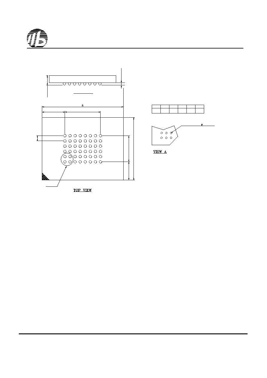
R0201-BS616UV1620
BSI
BS616UV1620
E0
.
1
3: SYMBOL "N" IS THE NUMBER OF SOLDER BALLS.
1: CONTROLLING DIMENSIONS ARE IN MILLIMETERS.
2: PIN#1 DOT MARKING BY LASER OR PAD PRINT.
N E
D
NOTES:
48
12.0
9.0
E1
D1
e
3.75
5.25
0.75
SIDE VIEW
D 0.1
D1
1.4 M
a
x
.
e
E1
0.25
0.05
SOLDER BALL 0.35 0.05
VIEW A
3.375
2.625
PACKAGE DIMENSIONS (continued)
48 mini-BGA (9 x 12mm)

Revision 2.2
April 2001
12
BSI
BS616UV1620
REVISION HISTORY
Revision
Description
Date
Note
2.2
2001 Data Sheet release
Apr. 15, 2001
R0201-BS616UV1620