 | –≠–ª–µ–∫—Ç—Ä–æ–Ω–Ω—ã–π –∫–æ–º–ø–æ–Ω–µ–Ω—Ç: ADC674 | –°–∫–∞—á–∞—Ç—å:  PDF PDF  ZIP ZIP |
Æ
Microprocessor-Compatible
ANALOG-TO-DIGITAL CONVERTER
FEATURES
q
COMPLETE 12-BIT A/D CONVERTER
WITH REFERENCE, CLOCK, AND 8-, 12-,
OR 16-BIT MICROPROCESSOR BUS
INTERFACE
q
IMPROVED PERFORMANCE SECOND
SOURCE FOR ADC574A/674A-TYPE A/D
CONVERTERS
Conversion Time: 15
µ
s max
Bus Access Time:150ns max
A
0
Input: Bus Contention During Read
Operation Eliminated
q
FULLY SPECIFIED FOR OPERATION ON
±
12V OR
±
15V SUPPLIES
q
NO MISSING CODES OVER
TEMPERATURE:
0
∞
C to +75
∞
C ADC674AJH, KH, JP, KP
Grades
≠55
∞
C to +125
∞
C (ADC674ASH, TH Grades)
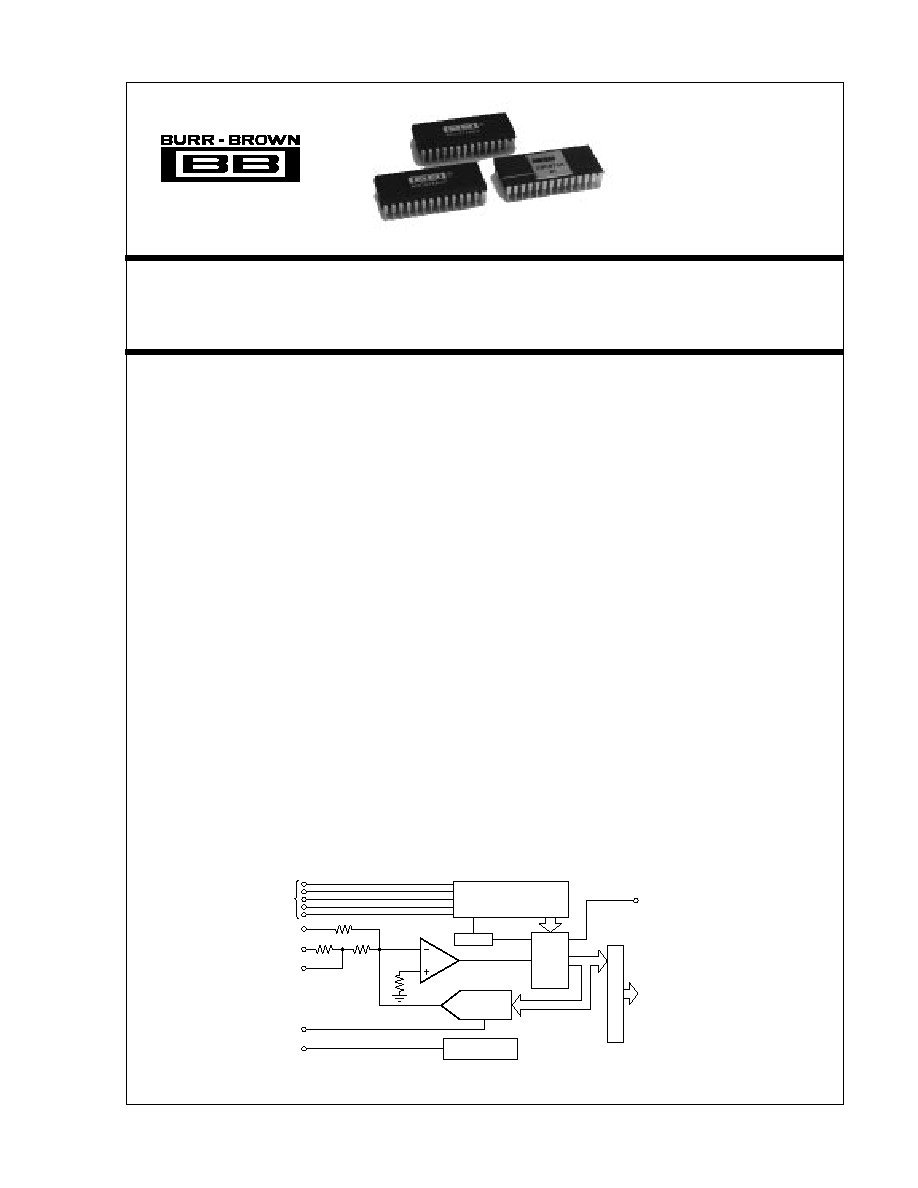
DESCRIPTION
The ADC674A is a 12-bit successive approximation
analog-to-digital converter, utilizing state-of-the-art
CMOS and laser-trimmed bipolar die custom-designed
for freedom from latch-up and for optimum AC per-
formance. It is complete with a self-contained +10V
reference, internal clock, digital interface for micro-
processor control, and three-state outputs.
The reference circuit, containing a buried zener, is
laser-trimmed for minimum temperature coefficient.
The clock oscillator is current-controlled for excel-
lent stability over temperature. Full-scale and offset
errors may be externally trimmed to zero. Internal
scaling resistors are provided for the selection of
analog input signal ranges of 0V to +10V, 0V to
+20V,
±
5V, and
±
10V.
The converter may be externally programmed to
provide 8- or 12-bit resolution. The conversion time
for 12 bits is factory set for 15
µ
s maximum.
Output data are available in a parallel format from
TTL-compatible three-state output buffers. Output data
are coded in straight binary for unipolar input signals
and bipolar offset binary for bipolar input signals.
The ADC674A, available in both industrial and
military temperature ranges, requires supply voltages
of +5V and
±
12V or
±
15V. It is packaged in a 28-pin
plastic DIP, or hermetic side-brazed ceramic DIP.
Control
Logic
Control
Inputs
Clock
Successive
Approximation
Register
12-Bit D/A
Converter
Comparator
Reference
Input
Reference
Output
Bipolar
Offset
20V Range
10V Range
10V
Reference
Three-State Buffers
Parallel
Data
Output
Status
International Airport Industrial Park ∑ Mailing Address: PO Box 11400 ∑ Tucson, AZ 85734 ∑ Street Address: 6730 S. Tucson Blvd. ∑ Tucson, AZ 85706
Tel: (520) 746-1111 ∑ Twx: 910-952-1111 ∑ Cable: BBRCORP ∑ Telex: 066-6491 ∑ FAX: (520) 889-1510 ∑ Immediate Product Info: (800) 548-6132
©
1984 Burr-Brown Corporation
PDS-551D
Printed in U.S.A. October, 1993
ADC674A
2
Æ
ADC674A
SPECIFICATIONS
ELECTRICAL
At T
A
= +25
∞
C, V
CC
=
±
12V or +15V, V
EE
= ≠12V or ≠15VDC, and V
LOGIC
= +5V, unless otherwise noted.
ADC674AJP, JH, SH
ADC674AKP, KH, TH
PARAMETER
MIN
TYP
MAX
MIN
TYP
MAX
UNITS
RESOULUTION
12
*
Bits
ANALOG INPUTS
Voltage Ranges: Unipolar
0 to +10, 0 to +20
*
V
Bipolar
±
5,
±
10
*
V
Impedance: 0 to +10V,
±
5V
4.7
5
5.3
*
*
*
k
±
10V, 0V to +20V
9.4
10
10.6
*
*
*
k
DIGITAL INPUTS (CE, CS, R/C, A
O
, 12/8)
Over Temperature Range
Voltages: Logic 1
+2
±
5.5
*
*
V
Logic 0
≠0.5
±
0.8
*
*
V
Current
≠5
0.2
±
5
*
*
*
µ
A
Capacitiance
5
*
pF
TRANSFER CHARACTERISTICS
ACCURACY
At +25
∞
C
±
1
±
1/2
LSB
Linearity Error
±
2
*
LSB
Unipolar Offset Error (adjustable to zero)
±
10
±
4
LSB
Bipolar Offset Error (adjustable to zero)
Full-Scale Calibration Error
(1)
(adjustable to zero)
±
0.25
*
% of FS
(2)
No Missing Codes Resolution (differential linearity)
11
±
1/2
12
Bits
Inherent Quantization Error
*
LSB
T
MIN
to T
MAX
Linearity Error: J, K Grades
±
1
±
1/2
LSB
S, T Grades
±
1
±
3/4
LSB
Full-Scale Calibration Error
Without Initial Adjustmen
(1)
: J, K Grades
±
0.47
±
0.37
% of FS
S, T Grades
±
0.75
±
0.5
% of FS
Adjusted to zero at +25
∞
C: J, K Grades
±
0.22
±
0.12
% of FS
S, T Grades
±
0.5
±
0.25
% of FS
No Missing Codes Resolution (differential linearity)
11
12
Bits
TEMPERATURE COEFFICIENTS (T
MIN
to T
MAX
)
(3)
Unipolar Offset: J, K Grades
±
10
±
5
ppm/
∞
C
S, T Grades
±
5
±
2.5
ppm/
∞
C
Max Change: All Grades
±
2
±
1
LSB
Bipolar Offset: All Grades
±
10
±
5
ppm/
∞
C
Max Change: J, K Grades
±
2
±
1
LSB
S, T Grades
±
4
±
2
LSB
Full-Scale Calibration: J, K Grades
±
45
±
25
ppm/
∞
C
S, T Grades
±
50
±
25
ppm/
∞
C
Max Change: J, K Grades
±
9
±
5
LSB
S, T Grades
±
20
±
10
LSB
POWER SENSITIVITY
Change in Full-Scale Calibration
+13.5V < V
CC
< +16.5V or +11.4V < V
CC
< +12.6V
±
2
±
1
LSB
+16.5V < V
EE
< +13.5V or ≠12.6V < V
EE
< ≠11.4V
±
2
±
1
LSB
+4.5V < V
LOGIC
< +5.5V
±
1/2
*
LSB
CONVERSION TIME
(4)
8-Bit Cycle
6
8
10
*
*
*
µ
s
12-Bit Cycle
9
12
15
*
*
*
µ
s
DIGITAL OUTPUT (DB
11
--DB
0
, Status)
(Over Temperature Range)
Outputs Codes: Unipolar
Bipolar
*
Logic Levels: Logic 0 (I
SINK
= 1.6mA)
+0.4
*
V
Logic 1 (I
SOURCE
= 500
µ
A)
+2.4
*
V
Leakage, Data Bits Only , High-Z State
≠5
0.1
+5
*
*
*
µ
A
Capacitance
5
*
pF
INTERNAL REFERENCE VOLTAGE
Voltage
+9.9
±
10
±
10.1
*
*
*
V
Source Current Available for External Loads
(5)
2
*
mA
Unipolar Straight Binary (USB)
Bipolar Offset Binary (BOB)

3
Æ
ADC674A
SPECIFICATIONS
(CONT)
ELECTRICAL
At T
A
= +25
∞
C, V
CC
=
±
12V or +15V, V
EE
= ≠12V or ≠15VDC, and V
LOGIC
= +5V, unless otherwise noted.
ADC674AJP, AJH, ASH
ADC674AKP, AKH, ATH
PARAMETER
MIN
TYP
MAX
MIN
TYP
MAX
UNITS
POWER SUPPLY REQUIREMENTS
Voltage: V
CC
+11.4
+16.5
*
*
V
V
EE
≠11.4
≠16.5
*
*
V
V
LOGIC
+4.5
+5.5
*
*
V
Current: I
CC
3.5
5
*
*
mA
I
EE
15
20
*
*
mA
I
LOGIC
9
15
*
*
mA
Power Dissipation (
±
15V Supplies)
325
450
*
*
mW
TEMPERATURE RANGE (Ambient: T
MIN
, T
MAX
)
Specification: K, J Grades
0
+75
*
*
∞
C
S, T Grades
≠55
+125
*
*
∞
C
Storage
≠65
+150
*
*
∞
C
* Specifications same as ADC674AJP, AJH, ASH.
NOTES: (1) With fixed 50
resistor from REF OUT to REF IN. This parameter is also adjustable to zero at +25
∞
C (see Optional External Full Scale and Offset
Adjustments section). (2) FS in this specification table means Full Scale Range. That is, for a
±
10V input range, FS means 20 V; for a 0 to +10V range, FS means
10V. The term Full Scale for these specifications instead of Full-Scale Range is used to be consistent with other vendor's 674A type specification tables. (3) Using
internal reference. (4) See Controlling the ADC674A section for detailed information concerning digital timing. (5) External loading must be constant during
conversion. The reference output requires no buffer amplifier with either
±
12V or
±
15V power supplies.
V
CC
to Digital Common .......................................................... 0 to +16.5V
V
EE
to Digital Common ........................................................... 0 to ≠16.5V
V
LOGIC
to Digital Common ........................................................... 0 to +7V
Analog Common to Digital Common ..................................................
±
1V
Control Inputs (CE, CS, A
O
, 12/8, R/C)
to Digital Common ............................................. ≠0.5V to V
LOGIC
+0.5V
Analog Inputs REF IN, BIP. OFF., 10V
IN
)
to Analog Common ......................................................................
±
16.5V
20V
IN
to Analog Common .................................................................
±
24V
REF OUT ...................................................... Indefinite Short to Common,
Momentary Short to V
CC
Max Junction Temperature ............................................................ +165
∞
C
Power Dissipation ........................................................................ 1000mW
Lead Temperature (soldering, 10s) ............................................... +300
∞
C
Thermal Resistance,
JA
: Ceramic ................................................. 50
∞
C/W
Plastic ................................................. 100
∞
C/W
CAUTION: These devices are sensitive to electrostatic discharge.
Appropriate I.C. handling procedures should be followed.
ABSOLUTE MAXIMUM RATINGS
BURN-IN SCREENING
Burn-in screening is available for both plastic and ceramic
package ADC674As. Burn-in duration is 160 hours at the
temperature (or equivalent combination of time and tem-
perature) indicated below:
Plastic "-BI" models: +85
∞
C
Ceramic "-BI" models: +125
∞
C
All units are 100% electrically tested after burn-in is com-
pleted. To order burn-in, add "-BI" to the base model
number (e.g., ADC674AKP-BI).
LINEARITY
TEMPERATURE
ERROR
MODEL
PACKAGE
RANGE
max (T
MIN
to T
MAX
)
ADC674AJP
Plastic DIP
0
∞
C to +75
∞
C
±
1LSB
ADC674AKP
Plastic DIP
0
∞
C to +75
∞
C
±
1/2LSB
ADC674AJH
Ceramic DIP
0
∞
C to +75
∞
C
±
1LSB
ADC674AKH
Ceramic DIP
0
∞
C to +75
∞
C
±
1/2LSB
ADC674ASH
Ceramic DIP
≠55
∞
C to +125
∞
C
±
1LSB
ADC674ATH
Ceramic DIP
≠55
∞
C to +125
∞
C
±
3/4LSB
ORDERING INFORMATION
BURN-IN SCREENING OPTION
See text for details.
BURN-IN
TEMPERATURE
TEMPERATURE
MODEL
PACKAGE
RANGE
(160 Hours)
(1)
ADC674AJP-BI
Plastic DIP
0
∞
C to +75
∞
C
+85
∞
C
ADC674AKP-BI
Plastic DIP
0
∞
C to +75
∞
C
+85
∞
C
ADC674AJH-BI
Ceramic DIP
0
∞
C to +75
∞
C
+125
∞
C
ADC674AKH-BI
Ceramic DIP
0
∞
C to +75
∞
C
+125
∞
C
ADC674ASH-BI
Ceramic DIP
≠55
∞
C to +125
∞
C
+125
∞
C
ADC674ATH-BI
Ceramic DIP
≠55
∞
C to +125
∞
C
+125
∞
C
NOTE: (1) Or equivalent combination of time and temperature.
PACKAGE INFORMATION
PACKAGE DRAWING
MODEL
PACKAGE
NUMBER
(1)
ADC674AJP
Plastic DIP
215
ADC674AKP
Plastic DIP
215
ADC674AJH
Ceramic DIP
149
ADC674AKH
Ceramic DIP
149
ADC674ASH
Ceramic DIP
149
ADC674ATH
Ceramic DIP
149
ADC674AJP-BI
Plastic DIP
215
ADC674AKP-BI
Plastic DIP
215
ADC674AJH-BI
Ceramic DIP
149
ADC674AKH-BI
Ceramic DIP
149
ADC674ASH-BI
Ceramic DIP
149
ADC674ATH-BI
Ceramic DIP
149
NOTE: (1) For detailed drawing and dimension table, please see end of data
sheet, or Appendix D of Burr-Brown IC Data Book.
4
Æ
ADC674A
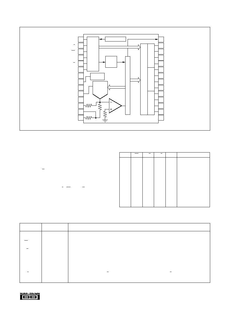
PIN CONFIGURATION
PIN
DESIGNATION
DEFINITION
FUNCTION
CE (Pin 6)
Chip Enable
Must be high ("1") to either initiate a conversion or read output data. 0-1 edge may be used to initiate a
(active high)
conversion.
CS (Pin 3)
Chip Select
Must be low ("0") ot either initiate a conversion or read output data. 1-0 edge may be used to initiate a conversion.
(active low)
R/C (Pin 5)
Read/Convert
Must be low ("0") to initiate either 8- or 12-bit conversions. 1-0 edge may be used to initiate a conversion. Must be high
("1" = read)
("1") to read output data. 0-1 edge may be used to initiate a read operation.
("0" = convert)
A
O
(Pin 4)
Byte Address
In the start-convert mode, A
O
selects 8-bit (A
O
= "1") or 12-bit (A
O
= "0") conversion mode. When reading output
Short Cycle
data in two 8-bit bytes, A
O
= "0" accesses
±
8MSBs (high byte) and A
O
= "1" accesses 4LSBs and trailing "0s" (low
byte).
12/8 (Pin 2)
Data Mode Select
When reading output data. 12/8 = "1" enables all 12 output bits simultaneously. 12/8 = "0" will enable the MSBs
("1" = 12-bits)
or LSBs as determined by the A
O
line.
("0" = 8-bits)
TABLE I. ADC674A Control Line Functions.
CONTROLLING THE ADC674A
The Burr-Brown ADC674A can be easily interfaced to most
microprocessor systems and other digital systems. The mi-
croprocessor may take full control of each conversion, or the
converter may operate in a stand-alone mode, controlled
only by the R/C input. Full control consists of selecting an
8- or 112-bit conversion cycle, initiating the conversion, and
the output data when ready--choosing either 12 bits all at
once, or 8 bits followed by 4 bits in a left-justified format.
The five control inputs (12/8, CS, A
O
, R/C, and CE) are all
TTL-/CMOS-compatible. The functions of the control in-
puts are described in Table I. The control function truth table
is listed in Table II.
CE
CS
R/C
12/8
A
O
OPERATION
0
X
X
X
X
None
X
1
X
X
X
None
0
0
X
0
Initiate 12-bit conversion
0
0
X
1
Initiate 8-bit conversion
1
0
X
0
Initiate 12-bit conversion
1
0
X
1
Initiate 8-bit conversion
1
0
X
0
Initiate 12-bit conversion
1
0
X
1
Initiate 8-bit conversion
1
0
1
1
X
Enable 12-bit output
1
0
1
0
0
Enable 8 MSBs only
1
0
1
0
1
Enable 4 LSBs plus 4
trailing zeros
TABLE II. Control Input Truth Table.
+5VDC Supply (V )
12/8
CS
A
R/C
CE
+V
Ref Out
Analog Common
Ref In
V
Bipolar Offset
10V Range
20V Range
Status
DB11 (MSB)
DB10
DB9
DB8
DB7
DB6
DB5
DB4
DB3
DB2
DB1
DB0 (LSB)
Digital Common
1
2
3
4
5
6
7
8
9
10
11
12
13
14
28
27
26
25
24
23
22
21
20
19
18
17
16
15
LOGIC
CC
EE
5k
10k
10V
Reference
12-Bit
D/A
Converter
Successive Approximation Register
Control
Logic
Power-up Reset
Clock
12 Bits
Comparator
12 Bits
Nibble A
Nibble B
Nibble C
Three-State Buffers and Control
O
5k

5
Æ
ADC674A
STAND-ALONE OPERATION
For stand-alone operation, control of the converter is accom-
plished by a single control line connected to R/C. In this
mode CS and A
O
are connected to digital common and CE
and 12/8 are connected to V
LOGIC
(+5V). The output data are
presented as 12-bit words. The stand-alone mode is used in
systems containing dedicated input ports which do not
require full bus interface capability.
Conversion is initiated by a high-to-low transition of R/C.
The three-state data output buffers are enabled when R/C is
high and STATUS is low. Thus, there are two possible
modes of operation; conversion can be initiated with either
positive or negative pulses. In either case, the R/C pulse
must remain low for a minimum of 50ns.
Figure 1 illustrates timing when conversion is initiated by an
R/C pulse which goes low and returns to the high state
during the conversion. In this case, the three-state outputs go
to the high-impedance state in response to the falling edge of
R/C and are enabled for external access of the data after
completion of the conversion. Figure 2 illustrates the timing
when conversion is initiated by a positive R/C pulse. In this
mode, the output data from the previous conversion is
enabled during the positive portion of R/C. A new conver-
sion is started on the falling edge of R/C, and the three-state
outputs return to the high impedance state until the next
occurrence of a high R/C pulse. Timing specifications for
stand-alone operation are listed in Table III.
FIGURE 2. R/C Pulse High--Outputs Enabled Only While
R/C is High.
FIGURE 1. R/C Pulse Low--Outputs Enabled After Con-
versions.
SYMBOL
PARAMETER
MIN
TYP
MAX
UNITS
t
HRL
Low R/C Pulse Width
50
ns
t
DS
STS Delay from R/C
200
ns
t
HDR
Data Valid After R/C Low
25
ns
t
HS
STS Delay After Data Valid
300
400
1000
ns
t
HRH
High R/C Pulse Width
150
ns
t
DDR
Data Access Time
150
ns
TABLE III. Stand-Alone Mode Timing.
FULLY CONTROLLED OPERATION
Conversion Length
Conversion length (8-bit or 12-bit) is determined by the state
of the A
O
input, which is latched upon receipt of a conver-
sion start transition (described below). If A
O
is latched high,
the conversion continues for 8 bits. The full 12-bit conver-
sion will occur if A
O
is low. If all 12 bits are read following
an 8-bit conversion the 3LSBs (DB0 - DB2) will be low
(logic 0) and DB3 will be high (logic 1). A
O
is latched because it is also involved in enabling the output
buffers. No other control inputs are latched.
CONVERSION START
The converter is commanded to initiate conversion by a
transition occurring on any of three logic inputs (CE, CS,
and R/C) as shown in Table II. Conversion is initiated by the
last of the three to reach the required state and thus all three
may be dynamically controlled. If necessary, all three may
change states simultaneously, and the nominal delay time is
the same regardless of which input actually starts conver-
sion. If it is desired that a particular input establish the actual
start of conversion, the other two should be stable a mini-
mum of 50ns prior to the transition of that input. Timing
relationships for start of conversion timing are illustrated in
Figure 3. The specifications for timing are contained in
Table IV.
FIGURE 3. Conversion Cycle Timing.
Data Valid
Data Valid
High-Z State
DB11-DB0
STATUS
R/C
t
HRL
t
DS
t
C
t
HS
t
HDR
Data Valid
High-Z State
DB11-DB0
STATUS
R/C
t
HRH
t
C
t
HDR
t
DDR
High-Z
t
DS
CE
t
SSC
t
HEC
CS
R/C
STATUS
t
C
DB11-DB0
A
O
t
SRC
t
HSC
t
HRC
t
SAC
t
HAC
t
DSC
High Impedance