 | –≠–ª–µ–∫—Ç—Ä–æ–Ω–Ω—ã–π –∫–æ–º–ø–æ–Ω–µ–Ω—Ç: ADC700BH | –°–∫–∞—á–∞—Ç—å:  PDF PDF  ZIP ZIP |
Æ
ADC700
16-Bit Resolution With Microprocessor Interface
A/D CONVERTER
DESCRIPTION
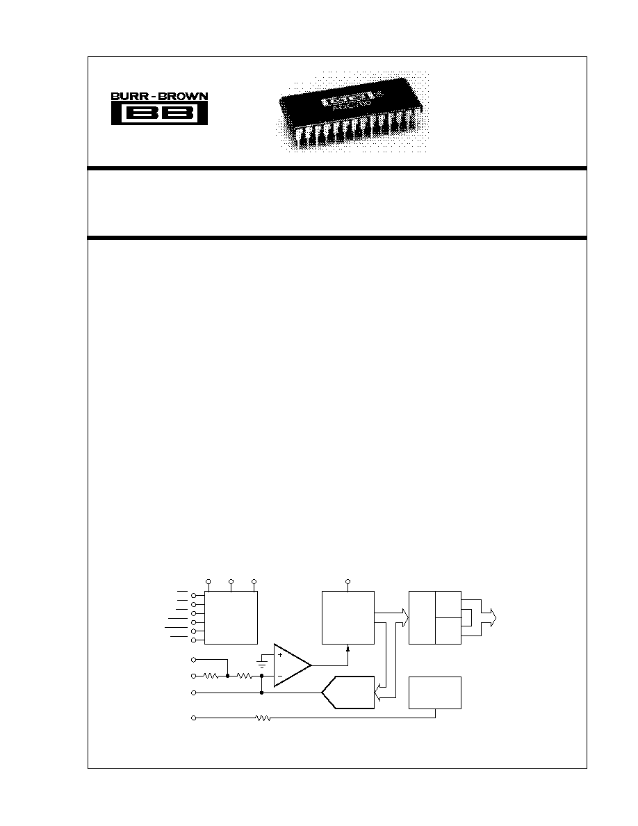
The ADC700 is a complete 16-bit resolution succes-
sive approximation analog-to-digital converter.
The reference circuit, containing a buried zener, is
laser-trimmed for minimum temperature coefficient.
The clock oscillator is current-controlled for excellent
stability over temperature. Gain and Zero errors may
be externally trimmed to zero. Analog input ranges of
0V to +5V, 0V to +10V, 0V to +20V,
±
2.5V,
±
5V, and
±
10V are available.
The conversion time is 17
µ
s max for a 16-bit conver-
sion over the three specification temperature ranges.
After a conversion, output data is stored in a latch
separate from the successive approximation logic. This
permits reading data during the next conversion, a
feature that provides flexible interface timing, espe-
cially for interrupt-driven interfaces.
Data is available in two 8-bit bytes from TTL-compat-
ible three-state output drivers. Output data is coded in
Straight Binary for unipolar input signals and Bipolar
Offset Binary or Twos complement for bipolar input
signals. BOB or BTC is selected by a logic function
available on one of the pins.
The ADC700 is available in commercial, industrial
and military temperature ranges. It is packaged in a
hermetic 28-pin side-braze ceramic DIP.
FEATURES
q
COMPLETE WITH REFERENCE, CLOCK,
8-BIT PORT MICROPROCESSOR
INTERFACE
q
CONVERSION TIME: 17
µ
s max
q
LINEARITY ERROR:
±
0.003% FSR max
q
NO MISSING CODES TO 14 BITS OVER
TEMPERATURE
q
SPECIFIED AT
±
12V AND
±
15V SUPPLIES
q
OUTPUT BUFFER LATCH FOR IMPROVED
INTERFACE TIMING FLEXIBILITY
q
PARALLEL AND SERIAL DATA OUTPUT
q
SMALL PACKAGE: 28-Pin DIP
Clock
and
Control Logic
CS
RD
WR
HBEN
BTCEN
Reset
Successive
Approximation
Register
Status
Serial Data
Strobe
Data
Ready
Serial Data
20V
10V
Analog
Inputs
Comparator
16-Bit
D/A
Converter
Data
Latch
16
16
3-
State
3-
State
8
Parallel
Data
Voltage
Reference
Bipolar
Offset
SJ
International Airport Industrial Park ∑ Mailing Address: PO Box 11400 ∑ Tucson, AZ 85734 ∑ Street Address: 6730 S. Tucson Blvd. ∑ Tucson, AZ 85706
Tel: (520) 746-1111 ∑ Twx: 910-952-1111 ∑ Cable: BBRCORP ∑ Telex: 066-6491 ∑ FAX: (520) 889-1510 ∑ Immediate Product Info: (800) 548-6132
© 1989 Burr-Brown Corporation
PDS-856A
Printed in U.S.A. October, 1993

2
Æ
ADC700
SPECIFICATIONS
ELECTRICAL
At T
A
= 25
∞
C and at rated supplies: V
DD
= +5V, +V
CC
= +12V or +15V, ≠V
CC
= ≠12V or ≠15V, unless otherwise noted.
ADC700JH,AH,RH
ADC700KH,BH,SH
CHARACTERISTICS
MIN
TYP
MAX
MIN
TYP
MAX
UNITS
RESOLUTION
16
*
Bits
ANALOG INPUTS
Voltage Ranges
Bipolar
±
2.5,
±
5,
±
10
*
V
Unipolar
0 to +5, 0 to +10, 0 to +20
*
V
Impedance (Direct Input)
0V to +5V,
±
2.5V
2.5
±
1%
*
k
0V to +10V,
±
5V
5
±
1%
*
k
0V to +20V,
±
10V
10
±
1%
*
k
DIGITAL SIGNALS (Over Specification Temperature Range)
Inputs
Logic Levels
(1)
V
IH
+2.0
+5.5
*
*
V
V
IL
0
+0.8
*
*
V
I
IH
(V
I
= +2.7V)
±
10
*
µ
A
I
IL
(V
I
= +0.4V)
±
20
*
µ
A
Outputs
Logic Levels
V
OL
(I
OL
= ≠1.6mA)
+0.4
*
V
V
OH
(I
OH
= +20
µ
A)
+2.4
*
V
I
LEAKAGE
Data Outputs Only, High Z
10
*
nA
TRANSFER CHARACTERISTICS
ACCURACY
Linearity Error
±
0.006
±
0.003
% of FSR
(2)
Differential Linearity Error
±
0.012
±
0.006
% of FSR
Gain Error
(3)
±
0.1
±
0.2
*
*
%
Zero Error
(3)
Bipolar Zero
±
0.1
±
0.2
*
*
% of FSR
Unipolar Zero
±
0.05
±
0.1
*
*
% of FSR
Noise at Transitions (3
p-p)
±
0.001
±
0.003
*
*
% of FSR
Power Supply Sensitivity
+V
CC
±
0.0015
*
%FSR/%V
CC
≠V
CC
±
0.0015
*
%FSR/%V
CC
V
DD
±
0.0005
*
%FSR/%V
DD
DRIFT (Over Specification Temperature Range)
Gain Drift
±
8
±
15
*
*
ppm/
∞
C
Zero Drift
Bipolar Zero
±
5
±
10
*
*
ppm of FSR/
∞
C
Unipolar Zero
±
2
±
4
*
*
ppm of FSR/
∞
C
Linearity Drift
±
1
±
3
*
±
2
ppm of FSR/
∞
C
No Missing Codes Temperature Range
JH (13-bit), KH (14-bit)
0
+70
*
*
∞
C
AH (13-bit), BH (14 bit)
≠25
+85
*
*
∞
C
RH (13-bit), SH (14-bit)
≠55
+125
*
*
∞
C
CONVERSION TIME 16 bits
15
17
*
*
µ
s
WARM≠UP TIME
5
*
min
OUTPUT DATA CODES
(4)
Unipolar Parallel
USB
*
Bipolar Parallel
(5)
BTC, BOB
*
Serial Output (NRZ)
USB, BOB
*
POWER SUPPLY REQUIREMENTS
Voltage Range
+V
CC
+11.4
+15
+16
*
*
*
VDC
≠V
CC
≠11.4
≠15
≠16
*
*
*
VDC
V
DD
+4.75
+5
+5.25
*
*
*
VDC
Current
(5)
+V
CC
+10
+15
*
*
mA
≠V
CC
≠28
≠35
*
*
mA
V
DD
+17
+20
*
*
mA
Power Dissipation
645
765
*
*
mW
TEMPERATURE RANGE
Specification
J, K Grades
0
+70
*
*
∞
C
A, B Grades
≠25
+85
*
*
∞
C
R, S Grades
≠55
+125
*
*
∞
C
Storage
≠65
+150
*
*
∞
C

3
Æ
ADC700
*Same specs as ADC700JH, AH, RH.
ORDERING INFORMATION
TEMPERATURE
LINEARITY
MODEL
RANGE
ERROR (%FSR)
1≠24
25≠99
100+
ADC700JH
0
∞
C to 70
∞
C
±
0.006
ADC700KH
0
∞
C to 70
∞
C
±
0.003
ADC700AH
≠25
∞
C to +85
∞
C
±
0.006
ADC700BH
≠25
∞
C to +85
∞
C
±
0.003
ADC700RH
≠55
∞
C to +125
∞
C
±
0.006
ADC700SH
≠55
∞
C to +125
∞
C
±
0.003
ABSOLUTE MAXIMUM RATINGS
+V
DD
to Digital Common ............................................................ 0V to +7V
+V
CC
to Analog Common ......................................................... 0V to +18V
≠V
CC
to Analog Common ......................................................... 0V to ≠18V
Digital Common to Analog Common ........................................ ≠1V to +1V
Digital Inputs to Digital Common ................................ ≠0.5V to V
DD
+ 0.5V
Analog Inputs .................................................................................. +16.5V
Power Dissipation ........................................................................ 1000mW
Storage Temperature ...................................................... ≠60
∞
C to +150
∞
C
Lead Temperature, (soldering, 10s) ............................................... +300
∞
C
NOTES: Stresses above those listed under "Absolute Maximum Ratings"
may cause permanent damage to the device. Exposure to absolute maxi-
mum rating conditions for extended periods may affect device reliability.
PACKAGING INFORMATION
PACKAGE DRAWING
MODEL
PACKAGE
NUMBER
(1)
ADC700JH
28-Pin Ceramic DIP
237
ADC700KH
28-Pin Ceramic DIP
237
ADC700AH
28-Pin Ceramic DIP
237
ADC700BH
28-Pin Ceramic DIP
237
ADC700RH
28-Pin Ceramic DIP
237
ADC700SH
28-Pin Ceramic DIP
237
NOTE: (1) For detailed drawing and dimension table, please see end of data
sheet, or Appendix D of Burr-Brown IC Data Book.
LIMIT AT
LIMIT AT
T
A
= 0, +70
∞
C
LIMIT AT
PARAMETER
T
A
= 25
∞
C
≠25
∞
C, +85
∞
C
T
A
= ≠55
∞
C, +125
∞
C
UNITS
DESCRIPTION
CONVERSION AND SERIAL DATA OUTPUT TIMING
t
1
0
0
0
ns, min
CS to WR Setup time
t
2
110
130
145
ns, max
WR to Status delay
t
3
40
40
40
ns, min
WR pulse width
t
4
0
0
0
ns, min
CS to WR Hold time
t
5
15
17
17
µ
s, max
Conversion time
t
6
550
600
650
ns, max
Data Ready to Status time
t
7
1100
1150
1250
ns, max
WR to first Serial Data Strobe
t
8
250
210
200
ns, min
First Serial Data to first Serial Data Strobe
t
9
310
360
400
ns, max
Last Serial Data Strobe to Status
t
10
0
0
0
ns, min
Status to WR Setup time
PARALLEL DATA OUTPUT TIMING
t
11
0
0
0
ns, min
HBEN to RD Setup time
t
12
0
0
0
ns, min
CS to RD Setup time
t
13
(7)
50
58
66
ns, max
High Byte Data Valid after RD
C
L
= 20pF (High Byte bus access time)
70
81
95
ns, max
High Byte Data Valid after RD
C
L
= 100pF (High Byte bus access time)
t
14
40
40
40
ns, min
RD pulse width
t
15
40
45
50
ns, max
Data Ready delay from RD (HBEN asserted)
t
16
(8)
50
60
65
ns, max
Data Hold time after RD (bus relinquish time)
t
17
0
0
0
ns, min
RD to CS Hold time
t
18
0
0
0
ns, min
RD to HBEN Hold time
RESET TIMING
t
19
60
70
80
ns, max
Data Ready low delay from Reset
t
20
70
81
95
ns, max
Status low delay from Reset
NOTES: (1) TTL, LSTTL, and 5V CMOS compatible. (2) FSR means Full Scale Range. For example, unit connected for
±
10V range has 20V FSR. (3) Externally
adjustable to zero. (4) See Table I. USB ≠ Unipolar Straight Binary; BTC ≠ Binary Two's Complement; BOB ≠ Bipolar Offset Binary; NRZ ≠ Non Return to Zero. (5)
Max supply current is specified at rated supply voltages. (6) All input control signals are specified with t
RISE
= t
FALL
= 5ns (10% to 90% of 5V) and timed from a voltage
level of 1.6V. (7) t
13
is measured with the load circuits of Figure 1 and defined as the time required for an output to cross 0.8V or 2.4V. (8) t
16
is defined as the time
required for the data lines to change 0.5V when loaded with the circuits of Figure 2.
TIMING SPECIFICATIONS
(6)
At V
DD
= +5V, +V
CC
= +12V or +15V, ≠V
CC
= ≠12V or ≠15V, unless otherwise noted.

4
Æ
ADC700
ADC700 Parallel Output Timing.
Start of Conversion and Serial Data Output Timing.
t
11
HBEN
Low
Byte
High
Byte
CS
RD
Parallel Data
Data Ready
t
18
t
11
t
17
t
12
t
17
t
12
t
13
t
16
t
13
t
16
DB8≠DB15
DB0≠DB7
t
15
t
14
t
14
ADC700 Reset Function Timing Diagram.
t
19
t
20
Reset
Data Ready
Status
The information provided herein is believed to be reliable; however, BURR-BROWN assumes no responsibility for inaccuracies or omissions. BURR-BROWN assumes
no responsibility for the use of this information, and all use of such information shall be entirely at the user's own risk. Prices and specifications are subject to change
without notice. No patent rights or licenses to any of the circuits described herein are implied or granted to any third party. BURR-BROWN does not authorize or warrant
any BURR-BROWN product for use in life support devices and/or systems.
t
10
t
3
t
1
t
4
CS
WR
Status
Data Ready
Serial Data Strobe
Serial Data
t
2
t
6
t
5
t
7
t
9
t
8
5
Æ
ADC700
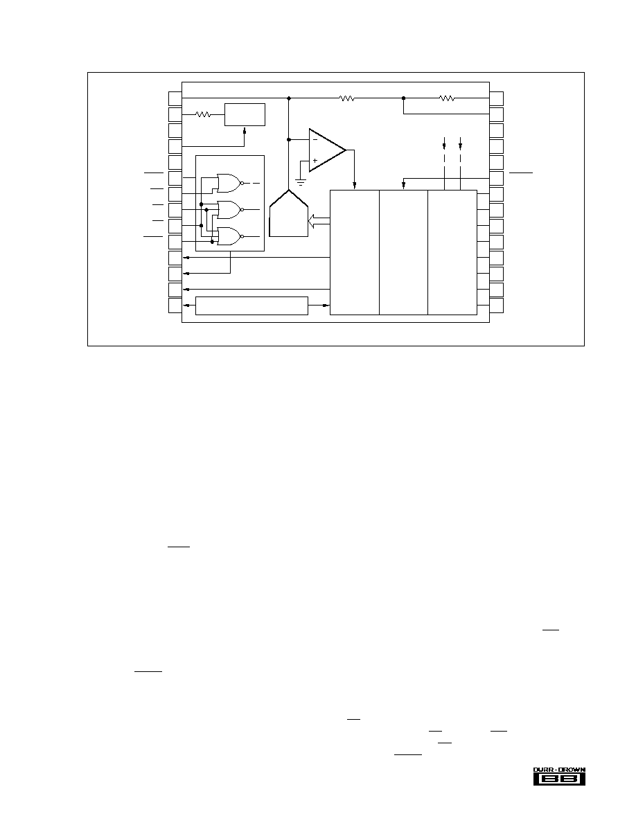
PIN CONFIGURATION
DESCRIPTION
AND OPERATING FEATURES
The ADC700 is a 16-bit resolution successive approxima-
tion A/D converter. Parallel digital data as well as serial data
is available. Several features have been included in the
ADC700 making it easier to interface with microprocessors
and/or serial data systems. Several analog input ranges are
available.
Some of the key operating features are described here. More
detail is given in later sections of the data sheet. Refer to the
block diagram above.
RESET
The ADC700 has a Reset input that must be asserted upon
power-up or after a power interruption. This initializes the
SAR, the output buffer register and Data Ready flag. Since
microprocessor systems already use a power-on reset circuit,
the same system reset signal can be used to initialize the
ADC700.
PARALLEL DATA
The parallel data output is available through an 8-bit port
with 3-state output drivers. High byte and low byte are
selected by HBEN (pin 10).
A buffer/latch is included between the successive approxi-
mation register (SAR) and the 3-state drivers. This feature
permits more flexible interface timing than is possible from
most successive approximation converters.
The "old" word can be read during the next conversion. A
Data Ready flag (pin 12) is asserted when a "new" word is
in the buffer register. The Data Ready flag goes low ("0")
when the most significant byte (high byte) is read. If the
"old" word is not read, or if only the least significant byte
(low byte) is read, Data Ready is not reset. The next
conversion output will overwrite the data latch when the
conversion is complete. The Data Ready flag remains high.
Refer to timing diagrams in the Specifications section.
SERIAL DATA
Sixteen-bit serial data output is available (pin 11) along with
a serial output strobe (pin 14). This serial data strobe is not
the internal SAR clock but is a special strobe for serial data
consisting of 16 negative-going edges (during conversion)
occurring about 200ns after each serial data bit is valid. This
feature eases the interface to shift registers or through opto-
couplers for applications requiring galvanic isolation.
STATUS
The familiar Status (or Busy) flag, present in successive
approximation A/D converters, is available (pin 13) and
indicates that a conversion is in progress. Status is valid
110ns after assertion of the convert command (WR low).
Status cannot be used as a sample-hold control because there
is not enough time for the sample-hold to settle to the
required error band before the ADC700 makes its first
conversion decision.
CHIP SELECT
CS (pin 9) selects the ADC700. No other functions can be
implemented unless CS is asserted. WR (pin 7) is the start-
of-conversion strobe. RD strobes each output data byte,
selected by HBEN (pin 10), to the 3-state drivers.
LSB
1
2
3
4
5
6
7
8
9
10
11
12
13
14
28
27
26
25
24
23
22
21
20
19
18
17
16
15
16-Bit
D/A
Converter
Successive
Approximation
Register
20V Range
10V Range
Analog Common
Digital Common
V
BTCEN
DB15/DB7
DB14/DB6
DB13/DB5
DB12/DB4
DB11/DB3
DB10/DB2
DB9/DB1
DB8/DB0
DD
Comparator In
Bipolar Offset
Gain Adjust
Reset
WR
RD
CS
HBEN
Serial Data
Data Ready
Status
Serial Data Strobe
CC
+V
CC
≠V
All internal control lines not shown. Refer to Figures 4 and 5 for Offset and Gain Adjust connections.
Data
Latch
3-State
Drivers
MSB LSB
Voltage
Reference
Clock and Clock Logic
5k
5k
MSB
Control Logic