 | –≠–ª–µ–∫—Ç—Ä–æ–Ω–Ω—ã–π –∫–æ–º–ø–æ–Ω–µ–Ω—Ç: ADC76A | –°–∫–∞—á–∞—Ç—å:  PDF PDF  ZIP ZIP |
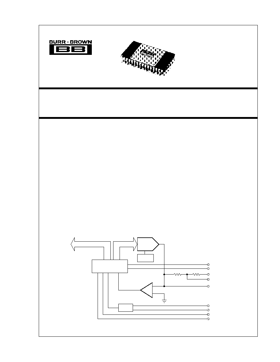
16-Bit
Successive Approx.
Register (SAR)
16-Bit D/A
Converter
Reference
Clock
≠
+
Parallel
Digital
Output
Short Cycle
Convert Command
}
Input Range
Select
Comparator In
Clock Rate Control
Clock Out
Status
Serial Out
16-Bit
ANALOG-TO-DIGITAL CONVERTER
International Airport Industrial Park ∑ Mailing Address: PO Box 11400 ∑ Tucson, AZ 85734 ∑ Street Address: 6730 S. Tucson Blvd. ∑ Tucson, AZ 85706
Tel: (520) 746-1111 ∑ Twx: 910-952-1111 ∑ Cable: BBRCORP ∑ Telex: 066-6491 ∑ FAX: (520) 889-1510 ∑ Immediate Product Info: (800) 548-6132
DESCRIPTION
The ADC76 is a high quality, 16-bit successive ap-
proximation analog-to-digital converter. The ADC76
uses state-of-the-art laser-trimmed IC thin-film resis-
tors and is packaged in a hermetic 32-pin dual-in-line
package. The converter is complete with internal ref-
erence, short cycling capabilities, serial output, and
thin-film scaling resistors, which allow selection of
analog input ranges of
±
2.5V,
±
5V,
±
10V, 0 to +5V,
0 to +10V and 0 to +20V.
It is specified for operation over two temperature
ranges: 0
∞
C to +70
∞
C (J, K) and ≠25
∞
C to +85
∞
C (A, B).
Data is available in parallel and serial form with
corresponding clock and status output. All digital
inputs and outputs are TTL-compatible.
Power supply voltages are
±
15VDC and +5VDC.
ADC76
FEATURES
q
16-BIT RESOLUTION
q
LINEARITY ERROR:
±
0.003% max (KG, BG)
q
NO MISSING CODES GUARANTEED
FROM ≠25
∞
C TO +85
∞
C
q
17
µ
s CONVERSION TIME (16-Bit)
q
SERIAL AND PARALLEL OUTPUTS
Æ
©
1990 Burr-Brown Corporation
PDS-1063A
Printed in U.S.A. December, 1993
Æ
ADC76
2
SPECIFICATIONS
ELECTRICAL
At +25
∞
C, and rated power supplies, unless otherwise noted.
ADC76J, K
ADC76A, B
MODEL
MIN
TYP
MAX
MIN
TYP
MAX
UNITS
RESOLUTION
16
*
Bits
ANALOG INPUTS
Voltage Ranges: Bipolar
±
2.5,
±
5,
±
10
*
V
Unipolar
0 to +5, 0 to +10
*
V
0 to +20
*
Impedance (Direct Input)
0 to +5V,
±
2.5V
2.5
*
k
0 to +10V,
±
5.0V
5
*
k
0 to +20V,
±
10V
10
*
k
DIGITAL INPUTS
(1)
Convert Command
Positive pulse 50ns wide (min) trailing edge ("1" to "0" initiates conversion)
Logic Loading
1
*
TTL Load
TRANSFER CHARACTERISTICS
ACCURACY
Gain Error
(2)
±
0.1
±
0.2
*
*
%
Offset Error: Unipolar
(2)
±
0.05
±
0.1
*
*
% of FSR
(3)
Bipolar
(2)
±
0.1
±
0.2
*
*
% of FSR
Linearity Error: K, B
±
0.003
*
% of FSR
J, A
±
0.006
*
% of FSR
Inherent Quantization Error
±
1/2
*
LSB
Differential Linearity Error
±
0.003
*
% of FSR
Noise (3
, p-p)
±
0.001
±
0.003
*
*
% of FSR
POWER SUPPLY SENSITIVITY
±
15VDC
0.003
*
% of FSR/%V
S
+5VDC
0.001
*
% of FSR/%V
S
CONVERSION TIME
(4)
14 Bits
15
*
µ
s
15 Bits
16
*
µ
s
16 Bits
17
*
µ
s
WARM-UP TIME
5
*
Min
DRIFT
Gain
±
15
*
ppm/
∞
C
Offset: Unipolar
±
2
±
4
*
*
ppm of FSR/
∞
C
Bipolar
±
10
*
ppm of FSR/
∞
C
Linearity
±
2
±
3
*
*
ppm of FSR/
∞
C
No Missing Codes Temp Range
J, A (13-bit)
0
+70
≠25
+85
∞
C
K, B (14-bit)
0
+70
≠25
+85
∞
C
OUTPUT DIGITAL DATA
(All codes complementary)
Parallel
Output Codes
(5)
: Unipolar
CSB
*
Bipolar
COB, CTC
(6)
*
Output Drive
2
*
TTL Loads
Serial Data Code (NRZ)
CSB, COB
*
Output Drive
2
*
TTL Loads
Status
Logic "1" during conversion
*
Status Output Drive
2
*
TTL Loads
Internal Clock: Clock Output Drive
2
*
TTL Loads
Frequency
(7)
933
1400
*
*
kHz
POWER SUPPLY REOUIREMENTS
Power Consumption
0.655
*
W
Rated Voltage: Analog
±
11.4
±
15
±
16
*
*
*
VDC
Digital
+4.75
+5
+5.25
*
*
*
VDC
Supply Drain: +15VDC
+10
+15
*
*
mA
≠15VDC
≠28
≠35
*
*
mA
+5VDC
+17
+20
*
*
mA
TEMPERATURE RANGE
Specification
0
+70
≠25
+85
∞
C
Storage
≠55
+125
*
*
∞
C
*Specification same as ADC76J, K.
NOTES: (1) CMOS/TTL compatible, i.e., Logic "0" = 0.8V, max, Logic "1" = 2.0V, min for inputs. For digital outputs Logic "0" = 0.4V, max, Logic "1' = 2.4V, min.
(2) Adjustable to zero. See "Optional External Gain and Offset Adjustment" section. (3) FSR means Full Scale Range. For example, unit connected for
±
10V range
has 20V FSR. (4) Conversion time may be shortened with "Short Cycle" set for lower resolution and with use of Clock Rate Control. See "Optional Conversion Time
Adjustment" section. The Clock Rate Control (pin 23) should be connected to Digital Common for specified conversion time. Short Cycle (pin 32) should be left open
for 16-bit resolution or connected to the n + 1 digital output for n-bit resolution. For example, connect Short Cycle to Bit 15 (pin 15) for 14-bit resolution. For resolutions
less than 16 bits, pin 32 should also be tied to +5V through a 2k
resistor. (5) See Table I. CSB = Complementary Straight Binary, COB = Complementary Offset
Binary, CTC = Complementary Two's Complement. (6) CTC coding obtained by inverting MSB (pin 1). (7) Adjustable with Clock Rate Control from approximately
933kHz to 1.4MHz.
Æ
ADC76
3
LINEARITY ERROR
MODEL
max (% of FSR)
TEMPERATURE RANGE
1-24
25-99
100-249
ADC76AG
±
0.006
≠25
∞
C to +85
∞
C
ADC76BG
±
0.003
≠25
∞
C to +85
∞
C
ADC76JG
±
0.006
0
∞
C to +70
∞
C
ADC76KG
±
0.003
0
∞
C to +70
∞
C
PIN CONFIGURATION
Top View
DIP
PACKAGE INFORMATION
PACKAGE DRAWING
MODEL
PACKAGE
NUMBER
(1)
ADC76JG
32-Pin Hermetic DIP
172-5
ADC76KG
32-Pin Hermetic DIP
172-5
ADC76AG
32-Pin Hermetic DIP
172-5
ADC76BG
32-Pin Hermetic DIP
172-5
NOTE: (1) For detailed drawing and dimension table, please see end of data
sheet, or Appendix D of Burr-Brown IC Data Book.
ABSOLUTE MAXIMUM SPECIFICATIONS
+V
CC
to Common .................................................................. 0V to +16.5V
≠V
CC
to Common .................................................................. 0V to ≠16.5V
+V
DD
to Common ....................................................................... 0V to +7V
Analog Common to Digital Common ...............................................
±
0.5V
Logic Inputs to Common ........................................................... 0V to V
DD
Maximum Power Dissipation ....................................................... 1000mW
Lead Temperature (soldering, 10s) ................................................. 300
∞
C
ORDERING INFORMATION
The information provided herein is believed to be reliable; however, BURR-BROWN assumes no responsibility for inaccuracies or omissions. BURR-BROWN assumes
no responsibility for the use of this information, and all use of such information shall be entirely at the user's own risk. Prices and specifications are subject to change
without notice. No patent rights or licenses to any of the circuits described herein are implied or granted to any third party. BURR-BROWN does not authorize or warrant
any BURR-BROWN product for use in life support devices and/or systems.
16-Bit D/A Converter
16-Bit SAR
5k
5k
6.3k
Reference
Clock
MSB Bit 1 1
Bit 2 2
Bit 3 3
Bit 4 4
Bit 5 5
Bit 6 6
Bit 7 7
Bit 8 8
Bit 9 9
Bit 10 10
Bit 11 11
Bit 12 12
(LSB for 13 Bits) Bit 13 13
Bit 15 15
(LSB for 14 Bits) Bit 14 14
Bit 16 16
≠
+
Comparator
32 Short Cycle
31 Convert Command
30 +5V Supply
29 Gain Adjust
28 +15V Supply
27 Comparator In
26 Bipolar Offset
25 10V
24 20V
23 Clock Rate Control
22 Analog Common
(1)
21 ≠15V Supply
20 Clock Out
18 Status
19 Digital Common
17 Serial Out
NOTE: (1) Metal lid is connected
to pin 22 (Analog Common).

Æ
ADC76
4
"0"
"1"
"1"
"0"
"0"
"1"
"1"
"1"
"0"
"1"
"1"
"0"
"1"
"0"
"0"
"1"
"1"
"0"
"0"
"0"
"1"
"1"
"1"
"1"
"1"
"1"
"0"
"0"
"0"
"1"
"1"
"0"
MSB
1
2
3
4
5
6
7
8
9
10
11
12
13
14
15
16
Maximum Throughput Time
Conversion Time
(2)
Convert Command
(1)
Internal Clock
Status (EOC)
MBS
Bit 2
Bit 3
Bit 4
Bit 5
Bit 6
Bit 7
Bit 8
Bit 9
Bit 10
Bit 11
Bit 12
Bit 13
Bit 14
Bit 15
Bit 16
Serial Data Out
NOTES: (1) The convert command must be at least 50ns wide and must remain low during a conversion. The conversion is
initiated by the "trailing edge" of the convert command. (2) 17
µ
s for 16 bits.
FIGURE 1. ADC76 Timing Diagram.
40-125ns
Bit 16
Status
Bit 16
Valid
FIGURE 2. Timing Relationship of Serial Data to Clock.
FIGURE 3. Timing Relationship of Valid Data to Status.
BINARY
(BIN) OUTPUT
INPUT VOLTAGE RANGE AND LSB VALUES
Analog Input
Voltage Range
Defined As:
±
10V
±
5V
±
2.5V
0 to +10V
0 to +5V
0 to +20V
Code
COB
(1)
COB
(1)
COB
(1)
Designation
or CTC
(2)
or CTC
(2)
or CTC
(2)
CSB
(3)
CSB
(3)
CSB
(3)
One Least
FSR
20V
10V
5V
10V
5V
20V
Significant
2
n
2
n
2
n
2
n
2
n
2
n
2
n
Bit (LSB)
n = 12
4.88mV
2.44mV
1.22mV
2.44mV
1.22mV
4.88mV
n = 13
2.44mV
1.22mV
610
µ
V
1.22mV
610
µ
V
2.44mV
n = 14
1.22mV
610
µ
V
305
µ
V
610
µ
V
305
µ
V
1.22mV
Transition Values
MSB LSB
000 ... 000
(4)
+Full Scale
+10V≠3/2LSB
+5V≠3/2LSB
+2.5V≠3/2LSB
+10V≠3/2LSB
+5V≠3/2LSB
+20V≠3/2LSB
011 ... 111
Mid Scale
0
0
0
+5V
+2.5V
+10V
111 ... 110
≠Full Scale
≠10V +1/2LSB
≠5V +1/2LSB
≠2.5V +1/2LSB
0 +1/2LSB
0 +1/2LSB
0 +1/2LSB
NOTES: (1) COB = Complementary Offset Binary. (2) Complementary Two's Complement--obtained by inverting the most significant bit MSB (pin 1).
(3) CSB = Complementary Straight Binary. (4) Voltages given are the nominal value for transition to the code specified.
Serial
Out
Clock
Out
40-125ns
40-125ns
TABLE I. Input Voltages, Transition Values, LSB Values, and Code Definitions.
Æ
ADC76
5
TYPICAL PERFORMANCE CURVES
T
A
= +25
∞
C, V
CC
=
±
15V unless otherwise noted.
FIGURE 1. Input vs Output for an Ideal Bipolar A/ D
Converter.
THEORY OF OPERATION
The accuracy of a successive approximation A/D converter
is described by the transfer function shown in Figure 1. All
successive approximation A/ D converters have an inherent
quantization error of
±
1/ 2LSB. The remaining errors in the
A/ D converter are combinations of analog errors due to the
linear circuitry, matching and tracking properties of the
ladder and scaling networks, power supply rejection, and
reference errors. In summary, these errors consist of initial
errors including Gain, Offset, Linearity, Differential Linear-
ity, and Power Supply Sensitivity. Initial Gain and Offset
errors may be adjusted to zero. Gain drift over temperature
rotates the line (Figure l) about the zero or minus full scale
point (all bits Off) and Offset drift shifts the line left or right
over the operating temperature range. Linearity error is
unadjustable and is the most meaningful indicator of A/ D
converter accuracy. Linearity error is the deviation of an
actual bit transition from the ideal transition value at any
level over the range of the A/ D converter. A differential
linearity error of
±
1/ 2LSB means that the width of each bit
step over the range of the A/ D converter is 1LSB,
±
1/ 2LSB.
The ADC76 is also monotonic, assuring that the output
digital code either increases or remains the same for increas-
ing analog input signals. Burr-Brown also guarantees that
this converter will have no missing codes over a specified
temperature range when short cycled for 14-bit operation
TIMING CONSIDERATIONS
The timing diagram in Figure 2 assumes an analog input
such that the positive true digital word 1001 1000 1001 0110
exists. The output will be complementary as shown in Figure
2 (0110 0111 0110 1001 is the digital output). Figures 3 and
4 are timing diagrams showing the relationship of serial data
to clock, and valid data to status.
DIGITAL CODES
Parallel Data
Two binary codes are available on the ADC76 parallel
output: they are complementary (logic "0" is true) straight
binary (CSB) for unipolar input signal ranges, and comple-
mentary offset binary (COB) for bipolar input signal ranges.
Complementary two's complement (CTC) may be obtained
by inverting the MSB (pin 1).
Table I shows the LSB, transition values, and code defini-
tions for each possible analog input signal range for 12-, 13-
and 14-bit resolutions. Figure 5 shows the connections for
14-bit resolution, parallel data output, with
±
10V input.
Serial Data
Two straight binary (complementary) codes are available on
the serial output line: CSB and COB. The serial data is
available only during conversion and appears with MSB
occurring first. The serial data is synchronous with the
internal clock as shown in the timing diagrams of Figures 2
and 3. The LSB and transition values shown in Table I also
apply to the serial data output except for the CTC code.
Analog Input
+FSR/2≠1LSB
e Off
+1/2LSB
IN
e On
IN
All Bits Off
≠FSR/2
Offset
Error
≠1/2LSB
Gain
Error
All Bit On
Digital Output (COB Code)*
0000 ... 0000
0000 ... 0001
0011 ... 1100
0011 ... 1110
0111 ... 1111
1000 ... 0000
1000 ... 0001
1111 ... 1110
1111 ... 1111
*See Table I for Digital Code Definitions.
≠25
+25
+85
Temperature (∞C)
+0.08
Gain Drift Error (% of FSR)
GAIN DRIFT ERROR (% OF FSR)
vs TEMPERATURE
+0.04
0
≠0.04
≠0.08
≠0.12
Frequency (Hz)
POWER SUPPLY REJECTION vs
SUPPLY RIPPLE FREQUENCY
% of FSR Error per % of Change In V
SUPPLY
0.1
0.06
0.04
0.02
0.01
0.006
0.004
0.002
0.001
+15VDC
+5VDC
≠15VDC
1
10
100
1k
10k
100k
NOTE: Pages
4&5 were
switched for
abridge version
for '96 data book.
Be sure to switch
back for full PDS.